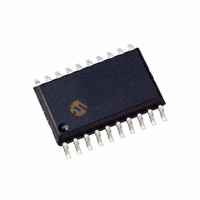
PIC18F13K22-I/SO Microchip Technology, PIC18F13K22-I/SO Datasheet - Page 80

PIC18F13K22-I/SO
Manufacturer Part Number
PIC18F13K22-I/SO
Description
IC MCU 8BIT 8KB FLASH 20SOIC
Manufacturer
Microchip Technology
Series
PIC® XLP™ 18Fr
Datasheets
1.PIC18LF13K22-ISS.pdf
(388 pages)
2.PIC18LF13K22-ISS.pdf
(12 pages)
3.PIC18F13K22-ISS.pdf
(382 pages)
Specifications of PIC18F13K22-I/SO
Program Memory Type
FLASH
Program Memory Size
8KB (4K x 16)
Package / Case
20-SOIC (7.5mm Width)
Core Processor
PIC
Core Size
8-Bit
Speed
64MHz
Connectivity
I²C, LIN, SPI, UART/USART
Peripherals
Brown-out Detect/Reset, POR, PWM, WDT
Number Of I /o
17
Eeprom Size
256 x 8
Ram Size
256 x 8
Voltage - Supply (vcc/vdd)
1.8 V ~ 5.5 V
Data Converters
A/D 12x10b
Oscillator Type
Internal
Operating Temperature
-40°C ~ 85°C
Processor Series
PIC18F
Core
PIC
Data Bus Width
8 bit
Data Ram Size
256 B
Interface Type
I2C, MSSP, SPI, USART
Maximum Clock Frequency
64 MHz
Number Of Programmable I/os
17
Number Of Timers
4
Operating Supply Voltage
1.8 V to 5.5 V
Maximum Operating Temperature
+ 125 C
Mounting Style
SMD/SMT
3rd Party Development Tools
52715-96, 52716-328, 52717-734, 52712-325, EWPIC18
Development Tools By Supplier
PG164130, DV164035, DV244005, DV164005
Minimum Operating Temperature
- 40 C
On-chip Adc
10 bit, 12 Channel
Package
20SOIC W
Device Core
PIC
Family Name
PIC18
Maximum Speed
64 MHz
A/d Bit Size
10 bit
A/d Channels Available
12
Height
2.05 mm
Length
12.8 mm
Supply Voltage (max)
5.5 V
Supply Voltage (min)
1.8 V, 2.7 V
Width
7.5 mm
Lead Free Status / RoHS Status
Lead free / RoHS Compliant
Lead Free Status / RoHS Status
Lead free / RoHS Compliant, Lead free / RoHS Compliant
Available stocks
Company
Part Number
Manufacturer
Quantity
Price
Company:
Part Number:
PIC18F13K22-I/SO
Manufacturer:
Microchip Technology
Quantity:
1 865
- Current page: 80 of 388
- Download datasheet (4Mb)
PIC18F1XK22/LF1XK22
This interrupt can wake the device from the Sleep mode,
or any of the Idle modes. The user, in the Interrupt
Service Routine, can clear the interrupt in the following
manner:
a)
b)
A mismatch condition will continue to set the RABIF flag
bit. Reading or writing PORTA will end the mismatch
condition and allow the RABIF bit to be cleared. The latch
holding the last read value is not affected by a MCLR nor
Brown-out Reset. After either one of these Resets, the
RABIF flag will continue to be set if a mismatch is present.
The interrupt-on-change feature is recommended for
wake-up on key depression operation and operations
where PORTA is only used for the interrupt-on-change
feature. Polling of PORTA is not recommended while
using the interrupt-on-change feature.
Each of the PORTA pins has an individually controlled
weak internal pull-up. When set, each bit of the WPUA
register enables the corresponding pin pull-up. When
cleared, the RABPU bit of the INTCON2 register
enables pull-ups on all pins which also have their cor-
responding WPUA bit set. When set, the RABPU bit
disables all weak pull-ups. The weak pull-up is auto-
matically turned off when the port pin is configured as
an output. The pull-ups are disabled on a Power-on
Reset.
RA3 is an input only pin. Its operation is controlled by
the MCLRE bit of the CONFIG3H register. When
selected as a port pin (MCLRE = 0), it functions as a
digital input only pin; as such, it does not have TRIS or
LAT bits associated with its operation.
DS41365D-page 80
Note:
Note 1: If a change on the I/O pin should occur
Any read or write of PORTA to clear the mis-
match condition (except when PORTA is the
source or destination of a MOVFF instruction).
Clear the flag bit, RABIF.
On a Power-on Reset, RA3 is enabled as
a digital input only if Master Clear
functionality is disabled.
when the read operation is being exe-
cuted (start of the Q2 cycle), then the
RABIF interrupt flag may not get set. Fur-
thermore, since a read or write on a port
affects all bits of that port, care must be
taken when using multiple pins in Inter-
rupt-on-change mode. Changes on one
pin may not be seen while servicing
changes on another pin.
Preliminary
Pins RA4 and RA5 are multiplexed with the main oscil-
lator pins; they are enabled as oscillator or I/O pins by
the selection of the main oscillator in the Configuration
register (see Section 22.1 “Configuration Bits” for
details). When they are not used as port pins, RA4 and
RA5 and their associated TRIS and LAT bits read as
‘0’.
RA<4,2:0> are pins multiplexed with analog inputs. The
operation of pins RA<4,2:0> as analog are selected by
setting the ANS<3:0> bits in the ANSEL register, which
is the default setting after a Power-on Reset.
EXAMPLE 8-1:
CLRF
CLRF
MOVLW
MOVWF
PORTA
LATA
030h
TRISA
; Initialize PORTA by
; clearing output
; data latches
; Alternate method
; to clear output
; data latches
; Value used to
; initialize data
; direction
; Set RA<5:4> as output
INITIALIZING PORTA
2010 Microchip Technology Inc.
Related parts for PIC18F13K22-I/SO
Image
Part Number
Description
Manufacturer
Datasheet
Request
R

Part Number:
Description:
Manufacturer:
Microchip Technology Inc.
Datasheet:

Part Number:
Description:
Manufacturer:
Microchip Technology Inc.
Datasheet:

Part Number:
Description:
Manufacturer:
Microchip Technology Inc.
Datasheet:

Part Number:
Description:
Manufacturer:
Microchip Technology Inc.
Datasheet:

Part Number:
Description:
Manufacturer:
Microchip Technology Inc.
Datasheet:

Part Number:
Description:
Manufacturer:
Microchip Technology Inc.
Datasheet:

Part Number:
Description:
Manufacturer:
Microchip Technology Inc.
Datasheet:

Part Number:
Description:
Manufacturer:
Microchip Technology Inc.
Datasheet:


