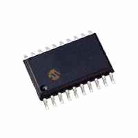
PIC18F13K22-I/SO Microchip Technology, PIC18F13K22-I/SO Datasheet - Page 47

PIC18F13K22-I/SO
Manufacturer Part Number
PIC18F13K22-I/SO
Description
IC MCU 8BIT 8KB FLASH 20SOIC
Manufacturer
Microchip Technology
Series
PIC® XLP™ 18Fr
Datasheets
1.PIC18LF13K22-ISS.pdf
(388 pages)
2.PIC18LF13K22-ISS.pdf
(12 pages)
3.PIC18F13K22-ISS.pdf
(382 pages)
Specifications of PIC18F13K22-I/SO
Program Memory Type
FLASH
Program Memory Size
8KB (4K x 16)
Package / Case
20-SOIC (7.5mm Width)
Core Processor
PIC
Core Size
8-Bit
Speed
64MHz
Connectivity
I²C, LIN, SPI, UART/USART
Peripherals
Brown-out Detect/Reset, POR, PWM, WDT
Number Of I /o
17
Eeprom Size
256 x 8
Ram Size
256 x 8
Voltage - Supply (vcc/vdd)
1.8 V ~ 5.5 V
Data Converters
A/D 12x10b
Oscillator Type
Internal
Operating Temperature
-40°C ~ 85°C
Processor Series
PIC18F
Core
PIC
Data Bus Width
8 bit
Data Ram Size
256 B
Interface Type
I2C, MSSP, SPI, USART
Maximum Clock Frequency
64 MHz
Number Of Programmable I/os
17
Number Of Timers
4
Operating Supply Voltage
1.8 V to 5.5 V
Maximum Operating Temperature
+ 125 C
Mounting Style
SMD/SMT
3rd Party Development Tools
52715-96, 52716-328, 52717-734, 52712-325, EWPIC18
Development Tools By Supplier
PG164130, DV164035, DV244005, DV164005
Minimum Operating Temperature
- 40 C
On-chip Adc
10 bit, 12 Channel
Package
20SOIC W
Device Core
PIC
Family Name
PIC18
Maximum Speed
64 MHz
A/d Bit Size
10 bit
A/d Channels Available
12
Height
2.05 mm
Length
12.8 mm
Supply Voltage (max)
5.5 V
Supply Voltage (min)
1.8 V, 2.7 V
Width
7.5 mm
Lead Free Status / RoHS Status
Lead free / RoHS Compliant
Lead Free Status / RoHS Status
Lead free / RoHS Compliant, Lead free / RoHS Compliant
Available stocks
Company
Part Number
Manufacturer
Quantity
Price
Company:
Part Number:
PIC18F13K22-I/SO
Manufacturer:
Microchip Technology
Quantity:
1 865
- Current page: 47 of 388
- Download datasheet (4Mb)
3.5.3
The use of Indexed Literal Offset Addressing mode
effectively changes how the first 96 locations of Access
RAM (00h to 5Fh) are mapped. Rather than containing
just the contents of the bottom section of Bank 0, this
mode maps the contents from a user defined “window”
that can be located anywhere in the data memory
space. The value of FSR2 establishes the lower bound-
ary of the addresses mapped into the window, while the
upper boundary is defined by FSR2 plus 95 (5Fh).
Addresses in the Access RAM above 5Fh are mapped
as previously described (see Section 3.3.2 “Access
Bank”). An example of Access Bank remapping in this
addressing mode is shown in Figure 3-10.
FIGURE 3-10:
2010 Microchip Technology Inc.
Example Situation:
Locations in the region
from the FSR2 pointer
(120h) to the pointer plus
05Fh (17Fh) are mapped
to
Access RAM (000h-05Fh).
Special File Registers at
F60h through FFFh are
mapped to 60h through
FFh, as usual.
Bank 0 addresses below
5Fh can still be addressed
by using the BSR.
ADDWF f, d, a
FSR2H:FSR2L = 120h
the
MAPPING THE ACCESS BANK IN
INDEXED LITERAL OFFSET MODE
bottom
of
REMAPPING THE ACCESS BANK WITH INDEXED LITERAL OFFSET
ADDRESSING
the
FFFh
17Fh
F00h
F60h
000h
100h
120h
200h
Data Memory
Window
Bank 14
Bank 15
Bank 0
through
Bank 1
Bank 1
Bank 2
SFRs
Preliminary
PIC18F1XK22/LF1XK22
Remapping of the Access Bank applies only to opera-
tions using the Indexed Literal Offset mode. Operations
that use the BSR (Access RAM bit is ‘1’) will continue
to use direct addressing as before.
3.6
Enabling the extended instruction set adds eight
additional commands to the existing PIC18 instruction
set. These instructions are executed as described in
Section 23.2 “Extended Instruction Set”.
PIC18 Instruction Execution and
the Extended Instruction Set
Bank 1 “Window”
Access Bank
SFRs
DS41365D-page 47
00h
5Fh
60h
FFh
Related parts for PIC18F13K22-I/SO
Image
Part Number
Description
Manufacturer
Datasheet
Request
R

Part Number:
Description:
Manufacturer:
Microchip Technology Inc.
Datasheet:

Part Number:
Description:
Manufacturer:
Microchip Technology Inc.
Datasheet:

Part Number:
Description:
Manufacturer:
Microchip Technology Inc.
Datasheet:

Part Number:
Description:
Manufacturer:
Microchip Technology Inc.
Datasheet:

Part Number:
Description:
Manufacturer:
Microchip Technology Inc.
Datasheet:

Part Number:
Description:
Manufacturer:
Microchip Technology Inc.
Datasheet:

Part Number:
Description:
Manufacturer:
Microchip Technology Inc.
Datasheet:

Part Number:
Description:
Manufacturer:
Microchip Technology Inc.
Datasheet:


