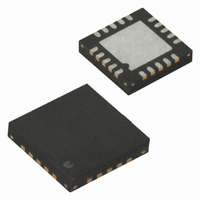
ATTINY24V-10MU Atmel, ATTINY24V-10MU Datasheet - Page 122

ATTINY24V-10MU
Manufacturer Part Number
ATTINY24V-10MU
Description
IC MCU AVR 2K FLASH 10MHZ 20-QFN
Manufacturer
Atmel
Series
AVR® ATtinyr
Specifications of ATTINY24V-10MU
Core Processor
AVR
Core Size
8-Bit
Speed
10MHz
Connectivity
USI
Peripherals
Brown-out Detect/Reset, POR, PWM, Temp Sensor, WDT
Number Of I /o
12
Program Memory Size
2KB (1K x 16)
Program Memory Type
FLASH
Eeprom Size
128 x 8
Ram Size
128 x 8
Voltage - Supply (vcc/vdd)
1.8 V ~ 5.5 V
Data Converters
A/D 8x10b
Oscillator Type
Internal
Operating Temperature
-40°C ~ 85°C
Package / Case
20-MLF®, QFN
Cpu Family
ATtiny
Device Core
AVR
Device Core Size
8b
Frequency (max)
10MHz
Interface Type
SPI/USI
Total Internal Ram Size
128Byte
# I/os (max)
12
Number Of Timers - General Purpose
2
Operating Supply Voltage (typ)
2.5/3.3/5V
Operating Supply Voltage (max)
5.5V
Operating Supply Voltage (min)
1.8V
On-chip Adc
8-chx10-bit
Instruction Set Architecture
RISC
Operating Temp Range
-40C to 85C
Operating Temperature Classification
Industrial
Mounting
Surface Mount
Pin Count
20
Package Type
MLF
Processor Series
ATTINY2x
Core
AVR8
Data Bus Width
8 bit
Data Ram Size
128 B
Maximum Clock Frequency
10 MHz
Number Of Programmable I/os
12
Number Of Timers
2
Maximum Operating Temperature
+ 85 C
Mounting Style
SMD/SMT
Minimum Operating Temperature
- 40 C
For Use With
ATSTK600-DIP40 - STK600 SOCKET/ADAPTER 40-PDIP770-1007 - ISP 4PORT ATMEL AVR MCU SPI/JTAGATAVRISP2 - PROGRAMMER AVR IN SYSTEMATSTK505 - ADAPTER KIT FOR 14PIN AVR MCU
Lead Free Status / RoHS Status
Lead free / RoHS Compliant
Available stocks
Company
Part Number
Manufacturer
Quantity
Price
Part Number:
ATTINY24V-10MU
Manufacturer:
ATMEL/爱特梅尔
Quantity:
20 000
- Current page: 122 of 238
- Download datasheet (5Mb)
122
ATtiny24/44/84
Figure 14-4. Two-wire Mode Operation, Simplified Diagram
The data direction is not given by the physical layer. A protocol, like the one used by the TWI-
bus, must be implemented to control the data flow.
Figure 14-5. Two-wire Mode, Typical Timing Diagram
Referring to the timing diagram
SDA
SCL
1. The start condition is generated by the master by forcing the SDA low line while keep-
2. In addition, the start detector will hold the SCL line low after the master has forced a
ing the SCL line high (A). SDA can be forced low either by writing a zero to bit 7 of the
USI Data Register, or by setting the corresponding bit in the PORTA register to zero.
Note that the Data Direction Register bit must be set to one for the output to be
enabled. The start detector logic of the slave device (see
detects the start condition and sets the USISIF Flag. The flag can generate an interrupt
if necessary.
negative edge on this line (B). This allows the slave to wake up from sleep or complete
other tasks before setting up the USI Data Register to receive the address. This is done
by clearing the start condition flag and resetting the counter.
SLAVE
MASTER
S
A B
Bit7
Bit7
Bit6
Bit6
C
ADDRESS
1 - 7
Bit5
Bit5
Bit4
Bit4
Bit3
Bit3
R/W
(Figure
8
D
Bit2
Bit2
Bit1
Bit1
14-5), a bus transfer involves the following steps:
ACK
9
Bit0
Bit0
E
DATA
1 - 8
Two-wire Clock
Control Unit
ACK
9
PORTxn
Figure 14-6 on page
HOLD
SCL
DATA
1 - 8
SDA
SCL
SDA
SCL
ACK
9
VCC
8006K–AVR–10/10
123)
F
P
Related parts for ATTINY24V-10MU
Image
Part Number
Description
Manufacturer
Datasheet
Request
R

Part Number:
Description:
IC MCU AVR 2K FLASH 10MHZ 14SOIC
Manufacturer:
Atmel
Datasheet:

Part Number:
Description:
IC MCU AVR 2K FLASH 10MHZ 14-DIP
Manufacturer:
Atmel
Datasheet:

Part Number:
Description:
MCU AVR 2KB FLASH 10MHZ 14SOIC
Manufacturer:
Atmel
Datasheet:

Part Number:
Description:
MCU AVR 2KB FLASH 10MHZ 20QFN
Manufacturer:
Atmel
Datasheet:

Part Number:
Description:
8-bit Avr Microcontroller With 2/4/8k Bytes Insystem Programmable Flash
Manufacturer:
ATMEL Corporation
Datasheet:

Part Number:
Description:
8-bit Microcontrollers - MCU Microcontroller
Manufacturer:
Atmel

Part Number:
Description:
Manufacturer:
Atmel Corporation
Datasheet:

Part Number:
Description:
Manufacturer:
Atmel Corporation
Datasheet:

Part Number:
Description:
IC MCU AVR 2K FLASH 20MHZ 20-QFN
Manufacturer:
Atmel
Datasheet:

Part Number:
Description:
IC MCU AVR 2K FLASH 20MHZ 14SOIC
Manufacturer:
Atmel
Datasheet:

Part Number:
Description:
MCU AVR 2K FLASH 15MHZ 20-QFN
Manufacturer:
Atmel
Datasheet:

Part Number:
Description:
IC MCU AVR 2K FLASH 20MHZ 14-DIP
Manufacturer:
Atmel
Datasheet:


