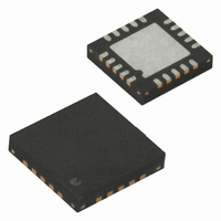
ATTINY45V-10MU Atmel, ATTINY45V-10MU Datasheet - Page 139

ATTINY45V-10MU
Manufacturer Part Number
ATTINY45V-10MU
Description
IC AVR MCU FLASH 4K 10MHZ 20MLF
Manufacturer
Atmel
Series
AVR® ATtinyr
Specifications of ATTINY45V-10MU
Core Processor
AVR
Core Size
8-Bit
Speed
10MHz
Connectivity
USI
Peripherals
Brown-out Detect/Reset, POR, PWM, WDT
Number Of I /o
6
Program Memory Size
4KB (2K x 16)
Program Memory Type
FLASH
Eeprom Size
256 x 8
Ram Size
256 x 8
Voltage - Supply (vcc/vdd)
1.8 V ~ 5.5 V
Data Converters
A/D 4x10b
Oscillator Type
Internal
Operating Temperature
-40°C ~ 85°C
Package / Case
20-MLF®, QFN
Processor Series
ATTINY4x
Core
AVR8
Data Bus Width
8 bit
Data Ram Size
256 B
Interface Type
USI
Maximum Clock Frequency
10 MHz
Number Of Programmable I/os
6
Number Of Timers
2
Operating Supply Voltage
1.8 V to 5.5 V
Maximum Operating Temperature
+ 85 C
Mounting Style
SMD/SMT
Minimum Operating Temperature
- 40 C
On-chip Adc
10 bit, 4 Channel
Package
20MLF EP
Device Core
AVR
Family Name
ATtiny
Maximum Speed
10 MHz
For Use With
ATSTK600-DIP40 - STK600 SOCKET/ADAPTER 40-PDIPATAVRBC100 - REF DESIGN KIT BATTERY CHARGER770-1007 - ISP 4PORT ATMEL AVR MCU SPI/JTAGATAVRDRAGON - KIT DRAGON 32KB FLASH MEM AVRATAVRISP2 - PROGRAMMER AVR IN SYSTEMATJTAGICE2 - AVR ON-CHIP D-BUG SYSTEM
Lead Free Status / RoHS Status
Lead free / RoHS Compliant
Available stocks
Company
Part Number
Manufacturer
Quantity
Price
Part Number:
ATTINY45V-10MU
Manufacturer:
ATMEL/爱特梅尔
Quantity:
20 000
- Current page: 139 of 236
- Download datasheet (5Mb)
2586M–AVR–07/10
• Bit 5 – ADLAR: ADC Left Adjust Result
The ADLAR bit affects the presentation of the ADC conversion result in the ADC Data Register.
Write one to ADLAR to left adjust the result. Otherwise, the result is right adjusted. Changing the
ADLAR bit will affect the ADC Data Register immediately, regardless of any ongoing conver-
sions. For a comple te description of this bit, see
on page
• Bits 3:0 – MUX[3:0]: Analog Channel and Gain Selection Bits
The value of these bits selects which combination of analog inputs are connected to the ADC. In
case of differential input (ADC0 - ADC1 or ADC2 - ADC3), gain selection is also made with these
bits. Selecting ADC2 or ADC0 as both inputs to the differential gain stage enables offset mea-
surements. Selecting the single-ended channel ADC4 enables the temperature sensor. Refer to
Table 17-4
effect until this conversion is complete (ADIF in ADCSRA is set).
Table 17-4.
1.
2.
MUX[3:0]
0101
0000
0001
0010
0100
1000
1001
1010
0011
0110
0111
1011
1100
1101
1110
1111
For offset calibration, only.
For temperature sensor.
141.
(1)
for details. If these bits are changed during a conversion, the change will not go into
Input Channel Selections
Single Ended
ADC0 (PB5)
ADC1 (PB2)
ADC2 (PB4)
ADC3 (PB3)
ADC4
Input
GND
N/A
V
N/A
BG
(2)
See “Operation” on page 127.
Differential Input
ADC2 (PB4)
ADC2 (PB4)
ADC2 (PB4)
ADC2 (PB4)
ADC0 (PB5)
ADC0 (PB5)
ADC0 (PB5)
ADC0 (PB5)
Positive
“ADCL and ADCH – The ADC Data Register”
Differential Input
ADC2 (PB4)
ADC2 (PB4)
ADC3 (PB3)
ADC3 (PB3)
ADC0 (PB5)
ADC0 (PB5)
ADC1 (PB2)
ADC1 (PB2)
Negative
N/A
N/A
Gain
20x
20x
20x
20x
1x
1x
1x
1x
139
Related parts for ATTINY45V-10MU
Image
Part Number
Description
Manufacturer
Datasheet
Request
R

Part Number:
Description:
IC AVR MCU 4K 10MHZ 8SOIC
Manufacturer:
Atmel
Datasheet:

Part Number:
Description:
MCU AVR 4KB FLASH 10MHZ 8SOIC
Manufacturer:
Atmel
Datasheet:

Part Number:
Description:
IC MCU AVR 4K FLASH 10MHZ 8TSSOP
Manufacturer:
Atmel
Datasheet:

Part Number:
Description:
IC AVR MCU 4K 10MHZ 8DIP
Manufacturer:
Atmel
Datasheet:

Part Number:
Description:
MCU AVR 4KB FLASH 10MHZ 8TSSOP
Manufacturer:
Atmel
Datasheet:

Part Number:
Description:
IC MCU AVR 4KB FLASH 20MHZ 8SOIC
Manufacturer:
Atmel
Datasheet:

Part Number:
Description:
MCU AVR 4KB FLASH 10MHZ 20QFN
Manufacturer:
Atmel
Datasheet:

Part Number:
Description:
IC AVR MCU 4K 10MHZ 8DIP
Manufacturer:
Atmel
Datasheet:

Part Number:
Description:
IC AVR MCU 4K 10MHZ 8SOIC
Manufacturer:
Atmel
Datasheet:

Part Number:
Description:
8-bit Microcontrollers - MCU 4K FL, 256B EESRAM, ADC,8 PINS - 10MHz
Manufacturer:
Atmel

Part Number:
Description:
Manufacturer:
Atmel Corporation
Datasheet:

Part Number:
Description:
Manufacturer:
Atmel Corporation
Datasheet:

Part Number:
Description:
IC AVR MCU 4K 20MHZ 8SOIC
Manufacturer:
Atmel
Datasheet:


