ATTINY85-20PU Atmel, ATTINY85-20PU Datasheet - Page 120
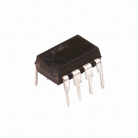
ATTINY85-20PU
Manufacturer Part Number
ATTINY85-20PU
Description
IC AVR MCU 8K 20MHZ 8DIP
Manufacturer
Atmel
Series
AVR® ATtinyr
Datasheets
1.ATTINY25-20MU.pdf
(236 pages)
2.ATTINY25-20PU.pdf
(30 pages)
3.ATTINY85-20PU.pdf
(234 pages)
Specifications of ATTINY85-20PU
Core Processor
AVR
Core Size
8-Bit
Speed
20MHz
Connectivity
USI
Peripherals
Brown-out Detect/Reset, POR, PWM, WDT
Number Of I /o
6
Program Memory Size
8KB (4K x 16)
Program Memory Type
FLASH
Eeprom Size
512 x 8
Ram Size
512 x 8
Voltage - Supply (vcc/vdd)
2.7 V ~ 5.5 V
Data Converters
A/D 4x10b
Oscillator Type
Internal
Operating Temperature
-40°C ~ 85°C
Package / Case
8-DIP (0.300", 7.62mm)
Processor Series
ATTINY8x
Core
AVR8
Data Bus Width
8 bit
Data Ram Size
512 B
Interface Type
USI
Maximum Clock Frequency
20 MHz
Number Of Programmable I/os
6
Number Of Timers
2
Operating Supply Voltage
2.7 V to 5.5 V
Maximum Operating Temperature
+ 85 C
Mounting Style
Through Hole
3rd Party Development Tools
EWAVR, EWAVR-BL
Development Tools By Supplier
ATAVRDRAGON, ATSTK500, ATSTK600, ATAVRISP2, ATAVRONEKIT
Minimum Operating Temperature
- 40 C
On-chip Adc
4-ch x 10-bit
Controller Family/series
AVR Tiny
No. Of I/o's
6
Eeprom Memory Size
512Byte
Ram Memory Size
512Byte
Cpu Speed
20MHz
No. Of Timers
2
Rohs Compliant
Yes
Cpu Family
ATtiny
Device Core
AVR
Device Core Size
8b
Frequency (max)
20MHz
Total Internal Ram Size
512Byte
# I/os (max)
6
Number Of Timers - General Purpose
2
Operating Supply Voltage (typ)
3.3/5V
Operating Supply Voltage (max)
5.5V
Operating Supply Voltage (min)
2.7V
Instruction Set Architecture
RISC
Operating Temp Range
-40C to 85C
Operating Temperature Classification
Industrial
Mounting
Through Hole
Pin Count
8
Package Type
PDIP
For Use With
ATSTK600 - DEV KIT FOR AVR/AVR32ATAVRBC100 - REF DESIGN KIT BATTERY CHARGER770-1007 - ISP 4PORT ATMEL AVR MCU SPI/JTAGATAVRDRAGON - KIT DRAGON 32KB FLASH MEM AVRATAVRISP2 - PROGRAMMER AVR IN SYSTEM
Lead Free Status / RoHS Status
Lead free / RoHS Compliant
Available stocks
Company
Part Number
Manufacturer
Quantity
Price
Company:

Part Number:
ATTINY85-20PU
Manufacturer:
CUI
Quantity:
1 000


15.5.4
120
ATtiny25/45/85
USICR – USI Control Register
The USI Control Register includes bits for interrupt enable, setting the wire mode, selecting the
clock and clock strobe.
• Bit 7 – USISIE: Start Condition Interrupt Enable
Setting this bit to one enables the start condition detector interrupt. If there is a pending interrupt
and USISIE and the Global Interrupt Enable Flag are set to one the interrupt will be executed
immediately. Refer to the USISIF bit description on
• Bit 6 – USIOIE: Counter Overflow Interrupt Enable
Setting this bit to one enables the counter overflow interrupt. If there is a pending interrupt and
USIOIE and the Global Interrupt Enable Flag are set to one the interrupt will be executed imme-
diately. Refer to the USIOIF bit description on
• Bits 5:4 – USIWM[1:0]: Wire Mode
These bits set the type of wire mode to be used, as shown in
Table 15-1.
Note:
Bit
0x0D
Read/Write
Initial Value
USIWM1
0
0
1
1
1. The DI and USCK pins are renamed to Serial Data (SDA) and Serial Clock (SCL) respectively
to avoid confusion between the modes of operation.
USIWM0
USISIE
Relationship between USIWM[1:0] and USI Operation
R/W
0
1
0
1
7
0
Description
Outputs, clock hold, and start detector disabled.
Port pins operates as normal.
Three-wire mode. Uses DO, DI, and USCK pins.
The Data Output (DO) pin overrides the corresponding bit in the PORTB register.
However, the corresponding DDRB bit still controls the data direction. When the port pin is
set as input the pin pull-up is controlled by the PORTB bit.
The Data Input (DI) and Serial Clock (USCK) pins do not affect the normal port operation.
When operating as master, clock pulses are software generated by toggling the PORTB
register, while the data direction is set to output. The USITC bit in the USICR Register can
be used for this purpose.
Two-wire mode. Uses SDA (DI) and SCL (USCK) pins
The Serial Data (SDA) and the Serial Clock (SCL) pins are bi-directional and use open-
collector output drives. The output drivers are enabled by setting the corresponding bit for
SDA and SCL in the DDRB register.
When the output driver is enabled for the SDA pin it will force the line SDA low if the
output of the USI Data Register or the corresponding bit in the PORTB register is zero.
Otherwise, the SDA line will not be driven (i.e., it is released). When the SCL pin output
driver is enabled the SCL line will be forced low if the corresponding bit in the PORTB
register is zero, or by the start detector. Otherwise the SCL line will not be driven.
The SCL line is held low when a start detector detects a start condition and the output is
enabled. Clearing the Start Condition Flag (USISIF) releases the line. The SDA and SCL
pin inputs is not affected by enabling this mode. Pull-ups on the SDA and SCL port pin are
disabled in Two-wire mode.
Two-wire mode. Uses SDA and SCL pins.
Same operation as in two-wire mode above, except that the SCL line is also held low
when a counter overflow occurs, and until the Counter Overflow Flag (USIOIF) is cleared.
USIOIE
R/W
6
0
USIWM1
R/W
5
0
USIWM0
R/W
4
0
page 119
page 119
USICS1
R/W
3
0
for further details.
Table 15-1
for further details.
USICS0
R/W
2
0
(1)
.
USICLK
below.
W
1
0
USITC
2586M–AVR–07/10
W
0
0
USICR
Related parts for ATTINY85-20PU
Image
Part Number
Description
Manufacturer
Datasheet
Request
R

Part Number:
Description:
Manufacturer:
Atmel Corporation
Datasheet:
Part Number:
Description:
Manufacturer:
Atmel Corporation
Datasheet:

Part Number:
Description:
IC AVR MCU 8K 20MHZ 8SOIC
Manufacturer:
Atmel
Datasheet:

Part Number:
Description:
IC MCU AVR 8K FLASH 20MHZ 20-QFN
Manufacturer:
Atmel
Datasheet:
Part Number:
Description:
MCU AVR 8K FLASH 15MHZ 8-SOIC
Manufacturer:
Atmel
Datasheet:

Part Number:
Description:
MCU AVR 8KB FLASH 20MHZ 8SOIC
Manufacturer:
Atmel
Datasheet:
Part Number:
Description:
IC MCU AVR 8KB FLASH 20MHZ 8SOIC
Manufacturer:
Atmel
Datasheet:
Part Number:
Description:
MCU AVR 8KB FLASH 20MHZ 20QFN
Manufacturer:
Atmel
Datasheet:

Part Number:
Description:
IC AVR MCU 8K 20MHZ 8DIP
Manufacturer:
Atmel
Datasheet:
Part Number:
Description:
IC AVR MCU 8K 20MHZ 8SOIC
Manufacturer:
Atmel
Datasheet: