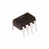
ATTINY85-20PU Atmel, ATTINY85-20PU Datasheet - Page 101

ATTINY85-20PU
Manufacturer Part Number
ATTINY85-20PU
Description
IC AVR MCU 8K 20MHZ 8DIP
Manufacturer
Atmel
Series
AVR® ATtinyr
Datasheets
1.ATTINY25-20MU.pdf
(236 pages)
2.ATTINY25-20PU.pdf
(30 pages)
3.ATTINY85-20PU.pdf
(234 pages)
Specifications of ATTINY85-20PU
Core Processor
AVR
Core Size
8-Bit
Speed
20MHz
Connectivity
USI
Peripherals
Brown-out Detect/Reset, POR, PWM, WDT
Number Of I /o
6
Program Memory Size
8KB (4K x 16)
Program Memory Type
FLASH
Eeprom Size
512 x 8
Ram Size
512 x 8
Voltage - Supply (vcc/vdd)
2.7 V ~ 5.5 V
Data Converters
A/D 4x10b
Oscillator Type
Internal
Operating Temperature
-40°C ~ 85°C
Package / Case
8-DIP (0.300", 7.62mm)
Processor Series
ATTINY8x
Core
AVR8
Data Bus Width
8 bit
Data Ram Size
512 B
Interface Type
USI
Maximum Clock Frequency
20 MHz
Number Of Programmable I/os
6
Number Of Timers
2
Operating Supply Voltage
2.7 V to 5.5 V
Maximum Operating Temperature
+ 85 C
Mounting Style
Through Hole
3rd Party Development Tools
EWAVR, EWAVR-BL
Development Tools By Supplier
ATAVRDRAGON, ATSTK500, ATSTK600, ATAVRISP2, ATAVRONEKIT
Minimum Operating Temperature
- 40 C
On-chip Adc
4-ch x 10-bit
Controller Family/series
AVR Tiny
No. Of I/o's
6
Eeprom Memory Size
512Byte
Ram Memory Size
512Byte
Cpu Speed
20MHz
No. Of Timers
2
Rohs Compliant
Yes
Cpu Family
ATtiny
Device Core
AVR
Device Core Size
8b
Frequency (max)
20MHz
Total Internal Ram Size
512Byte
# I/os (max)
6
Number Of Timers - General Purpose
2
Operating Supply Voltage (typ)
3.3/5V
Operating Supply Voltage (max)
5.5V
Operating Supply Voltage (min)
2.7V
Instruction Set Architecture
RISC
Operating Temp Range
-40C to 85C
Operating Temperature Classification
Industrial
Mounting
Through Hole
Pin Count
8
Package Type
PDIP
For Use With
ATSTK600 - DEV KIT FOR AVR/AVR32ATAVRBC100 - REF DESIGN KIT BATTERY CHARGER770-1007 - ISP 4PORT ATMEL AVR MCU SPI/JTAGATAVRDRAGON - KIT DRAGON 32KB FLASH MEM AVRATAVRISP2 - PROGRAMMER AVR IN SYSTEM
Lead Free Status / RoHS Status
Lead free / RoHS Compliant
Available stocks
Company
Part Number
Manufacturer
Quantity
Price
Company:
Part Number:
ATTINY85-20PU
Manufacturer:
CUI
Quantity:
1 000
13.2.1
2586M–AVR–07/10
Timer/Counter1 in PWM Mode
When the PWM mode is selected, Timer/Counter1 and the Output Compare Register A -
OCR1A form an 8-bit, free-running and glitch-free PWM generator with output on the
PB1(OC1A).
When the counter value match the content of OCR1A, the OC1A and output is set or cleared
according to the COM1A1/COM1A0 bits in the Timer/Counter1 Control Register A - TCCR1, as
shown in
Timer/Counter1 acts as an up-counter, counting from $00 up to the value specified in the output
compare register OCR1C, and starting from $00 up again. A compare match with OCR1C will
set an overflow interrupt flag (TOV1) after a synchronization delay following the compare event.
Table 13-1.
Note that in PWM mode, writing to the Output Compare Register OCR1A, the data value is first
transferred to a temporary location. The value is latched into OCR1A when the Timer/Counter
reaches OCR1C. This prevents the occurrence of odd-length PWM pulses (glitches) in the event
of an unsynchronized OCR1A. See
Figure 13-4. Effects of Unsynchronized OCR Latching
During the time between the write and the latch operation, a read from OCR1A will read the con-
tents of the temporary location. This means that the most recently written value always will read
out of OCR1A.
COM1A1
0
0
1
1
Unsynchronized OC1A Latch
Table
Synchronized OC1A Latch
Compare Mode Select in PWM Mode
COM1A0
13-1.
0
1
0
1
Effect on Output Compare Pin
OC1A not connected.
OC1A not connected.
OC1A cleared on compare match. Set when TCNT1 = $00.
OC1A set on compare match. Cleared when TCNT1 = $00.
Figure 13-4
Glitch
for an e xample.
Compare Value changes
Compare Value changes
Counter Value
Compare Value
PWM Output OC1A
Counter Value
Compare Value
PWM Output OC1A
101


