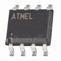
ATTINY85-20SU Atmel, ATTINY85-20SU Datasheet - Page 92

ATTINY85-20SU
Manufacturer Part Number
ATTINY85-20SU
Description
IC AVR MCU 8K 20MHZ 8SOIC
Manufacturer
Atmel
Series
AVR® ATtinyr
Specifications of ATTINY85-20SU
Core Processor
AVR
Core Size
8-Bit
Speed
20MHz
Connectivity
USI
Peripherals
Brown-out Detect/Reset, POR, PWM, WDT
Number Of I /o
6
Program Memory Size
8KB (4K x 16)
Program Memory Type
FLASH
Eeprom Size
512 x 8
Ram Size
512 x 8
Voltage - Supply (vcc/vdd)
2.7 V ~ 5.5 V
Data Converters
A/D 4x10b
Oscillator Type
Internal
Operating Temperature
-40°C ~ 85°C
Package / Case
8-SOIC (5.3mm Width), 8-SOP, 8-SOEIAJ
Processor Series
ATTINY8x
Core
AVR8
Data Bus Width
8 bit
Data Ram Size
512 B
Interface Type
USI
Maximum Clock Frequency
20 MHz
Number Of Programmable I/os
6
Number Of Timers
2
Operating Supply Voltage
2.7 V to 5.5 V
Maximum Operating Temperature
+ 85 C
Mounting Style
SMD/SMT
3rd Party Development Tools
EWAVR, EWAVR-BL
Development Tools By Supplier
ATAVRDRAGON, ATSTK500, ATSTK600, ATAVRISP2, ATAVRONEKIT
Minimum Operating Temperature
- 40 C
On-chip Adc
4-ch x 10-bit
For Use With
ATSTK600-DIP40 - STK600 SOCKET/ADAPTER 40-PDIPATAVRBC100 - REF DESIGN KIT BATTERY CHARGER770-1007 - ISP 4PORT ATMEL AVR MCU SPI/JTAG770-1004 - ISP 4PORT FOR ATMEL AVR MCU SPIATAVRDRAGON - KIT DRAGON 32KB FLASH MEM AVRATAVRISP2 - PROGRAMMER AVR IN SYSTEM
Lead Free Status / RoHS Status
Lead free / RoHS Compliant
Available stocks
Company
Part Number
Manufacturer
Quantity
Price
Part Number:
ATTINY85-20SU
Manufacturer:
ATMEL/爱特梅尔
Quantity:
20 000
- Current page: 92 of 236
- Download datasheet (5Mb)
12.3
12.3.1
92
Register Description
ATtiny25/45/85
TCCR1 – Timer/Counter1 Control Register
• Bit 7 – CTC1 : Clear Timer/Counter on Compare Match
When the CTC1 control bit is set (one), Timer/Counter1 is reset to $00 in the CPU clock cycle
after a compare match with OCR1C register value. If the control bit is cleared, Timer/Counter1
continues counting and is unaffected by a compare match.
• Bit 6 – PWM1A: Pulse Width Modulator A Enable
When set (one) this bit enables PWM mode based on comparator OCR1A in Timer/Counter1
and the counter value is reset to $00 in the CPU clock cycle after a compare match with OCR1C
register value.
• Bits 5:4 – COM1A[1:0]: Comparator A Output Mode, Bits 1 and 0
The COM1A1 and COM1A0 control bits determine any output pin action following a compare
match with compare register A in Timer/Counter1. Since the output pin action is an alternative
function to an I/O port, the corresponding direction control bit must be set (one) in order to con-
trol an output pin.
In Normal mode, the COM1A1 and COM1A0 control bits determine the output pin actions that
affect pin PB1 (OC1A) as described in
mode.
Table 12-4.
In PWM mode, these bits have different functions. Refer to
description.
Bit
0x30
Read/Write
Initial value
COM1A1
0
0
1
1
CTC1
Comparator A Mode Select
R/W
COM1A0
7
0
0
1
0
1
PWM1A
R/W
6
0
Description
Timer/Counter Comparator A disconnected from output pin OC1A.
Toggle the OC1A output line.
Clear the OC1A output line.
Set the OC1A output line
COM1A1
R/W
5
0
Table
COM1A0
R/W
4
0
12-4. Note that OC1A is not connected in normal
CS13
R/W
3
0
Table 12-1 on page 89
CS12
R/W
2
0
CS11
R/W
1
0
CS10
R/W
0
0
2586M–AVR–07/10
for a detailed
TCCR1
Related parts for ATTINY85-20SU
Image
Part Number
Description
Manufacturer
Datasheet
Request
R

Part Number:
Description:
Manufacturer:
Atmel Corporation
Datasheet:

Part Number:
Description:
Manufacturer:
Atmel Corporation
Datasheet:

Part Number:
Description:
IC MCU AVR 8K FLASH 20MHZ 20-QFN
Manufacturer:
Atmel
Datasheet:

Part Number:
Description:
IC AVR MCU 8K 20MHZ 8DIP
Manufacturer:
Atmel
Datasheet:

Part Number:
Description:
MCU AVR 8K FLASH 15MHZ 8-SOIC
Manufacturer:
Atmel
Datasheet:

Part Number:
Description:
MCU AVR 8KB FLASH 20MHZ 8SOIC
Manufacturer:
Atmel
Datasheet:

Part Number:
Description:
IC MCU AVR 8KB FLASH 20MHZ 8SOIC
Manufacturer:
Atmel
Datasheet:

Part Number:
Description:
MCU AVR 8KB FLASH 20MHZ 20QFN
Manufacturer:
Atmel
Datasheet:

Part Number:
Description:
IC AVR MCU 8K 20MHZ 8DIP
Manufacturer:
Atmel
Datasheet:

Part Number:
Description:
IC AVR MCU 8K 20MHZ 8SOIC
Manufacturer:
Atmel
Datasheet:


