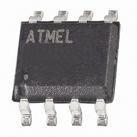
ATTINY85-20SU Atmel, ATTINY85-20SU Datasheet - Page 16

ATTINY85-20SU
Manufacturer Part Number
ATTINY85-20SU
Description
IC AVR MCU 8K 20MHZ 8SOIC
Manufacturer
Atmel
Series
AVR® ATtinyr
Specifications of ATTINY85-20SU
Core Processor
AVR
Core Size
8-Bit
Speed
20MHz
Connectivity
USI
Peripherals
Brown-out Detect/Reset, POR, PWM, WDT
Number Of I /o
6
Program Memory Size
8KB (4K x 16)
Program Memory Type
FLASH
Eeprom Size
512 x 8
Ram Size
512 x 8
Voltage - Supply (vcc/vdd)
2.7 V ~ 5.5 V
Data Converters
A/D 4x10b
Oscillator Type
Internal
Operating Temperature
-40°C ~ 85°C
Package / Case
8-SOIC (5.3mm Width), 8-SOP, 8-SOEIAJ
Processor Series
ATTINY8x
Core
AVR8
Data Bus Width
8 bit
Data Ram Size
512 B
Interface Type
USI
Maximum Clock Frequency
20 MHz
Number Of Programmable I/os
6
Number Of Timers
2
Operating Supply Voltage
2.7 V to 5.5 V
Maximum Operating Temperature
+ 85 C
Mounting Style
SMD/SMT
3rd Party Development Tools
EWAVR, EWAVR-BL
Development Tools By Supplier
ATAVRDRAGON, ATSTK500, ATSTK600, ATAVRISP2, ATAVRONEKIT
Minimum Operating Temperature
- 40 C
On-chip Adc
4-ch x 10-bit
For Use With
ATSTK600-DIP40 - STK600 SOCKET/ADAPTER 40-PDIPATAVRBC100 - REF DESIGN KIT BATTERY CHARGER770-1007 - ISP 4PORT ATMEL AVR MCU SPI/JTAG770-1004 - ISP 4PORT FOR ATMEL AVR MCU SPIATAVRDRAGON - KIT DRAGON 32KB FLASH MEM AVRATAVRISP2 - PROGRAMMER AVR IN SYSTEM
Lead Free Status / RoHS Status
Lead free / RoHS Compliant
Available stocks
Company
Part Number
Manufacturer
Quantity
Price
Part Number:
ATTINY85-20SU
Manufacturer:
ATMEL/爱特梅尔
Quantity:
20 000
- Current page: 16 of 236
- Download datasheet (5Mb)
5.2.1
5.3
16
EEPROM Data Memory
ATtiny25/45/85
Data Memory Access Times
When using register indirect addressing modes with automatic pre-decrement and post-incre-
ment, the address registers X, Y, and Z are decremented or incremented.
The 32 general purpose working registers, 64 I/O Registers, and the 128/256/512 bytes of inter-
nal data SRAM in the ATtiny25/45/85 are all accessible through all these addressing modes.
The Register File is described in
Figure 5-2.
This section describes the general access timing concepts for internal memory access. The
internal data SRAM access is performed in two clk
Figure 5-3.
The ATtiny25/45/85 contains 128/256/512 bytes of data EEPROM memory. It is organized as a
separate data space, in which single bytes can be read and written. The EEPROM has an
endurance of at least 100,000 write/erase cycles. The access between the EEPROM and the
CPU is described in the following, specifying the EEPROM Address Registers, the EEPROM
Data Register, and the EEPROM Control Register. For details see
155.
Data Memory Map
On-chip Data SRAM Access Cycles
Address
clk
Data
Data
WR
CPU
RD
(128/256/512 x 8)
64 I/O Registers
Data Memory
Internal SRAM
Compute Address
32 Registers
“General Purpose Register File” on page
T1
Memory Access Instruction
0x0DF/0x015F/0x025F
0x0000 - 0x001F
0x0020 - 0x005F
0x0060
Address valid
CPU
T2
cycles as described in
Next Instruction
“Serial Downloading” on page
T3
10.
Figure
2586M–AVR–07/10
5-3.
Related parts for ATTINY85-20SU
Image
Part Number
Description
Manufacturer
Datasheet
Request
R

Part Number:
Description:
Manufacturer:
Atmel Corporation
Datasheet:

Part Number:
Description:
Manufacturer:
Atmel Corporation
Datasheet:

Part Number:
Description:
IC MCU AVR 8K FLASH 20MHZ 20-QFN
Manufacturer:
Atmel
Datasheet:

Part Number:
Description:
IC AVR MCU 8K 20MHZ 8DIP
Manufacturer:
Atmel
Datasheet:

Part Number:
Description:
MCU AVR 8K FLASH 15MHZ 8-SOIC
Manufacturer:
Atmel
Datasheet:

Part Number:
Description:
MCU AVR 8KB FLASH 20MHZ 8SOIC
Manufacturer:
Atmel
Datasheet:

Part Number:
Description:
IC MCU AVR 8KB FLASH 20MHZ 8SOIC
Manufacturer:
Atmel
Datasheet:

Part Number:
Description:
MCU AVR 8KB FLASH 20MHZ 20QFN
Manufacturer:
Atmel
Datasheet:

Part Number:
Description:
IC AVR MCU 8K 20MHZ 8DIP
Manufacturer:
Atmel
Datasheet:

Part Number:
Description:
IC AVR MCU 8K 20MHZ 8SOIC
Manufacturer:
Atmel
Datasheet:


