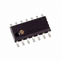
PIC16F616-I/SL Microchip Technology, PIC16F616-I/SL Datasheet - Page 68

PIC16F616-I/SL
Manufacturer Part Number
PIC16F616-I/SL
Description
IC PIC MCU FLASH 2KX14 14SOIC
Manufacturer
Microchip Technology
Series
PIC® 16Fr
Datasheets
1.PIC12F609T-ISN.pdf
(26 pages)
2.PIC16F616T-ISL.pdf
(4 pages)
3.PIC16F616T-ISL.pdf
(214 pages)
4.PIC16F616T-ISL.pdf
(8 pages)
5.PIC16F616-ESL.pdf
(180 pages)
Specifications of PIC16F616-I/SL
Program Memory Type
FLASH
Program Memory Size
3.5KB (2K x 14)
Package / Case
14-SOIC (3.9mm Width), 14-SOL
Core Processor
PIC
Core Size
8-Bit
Speed
20MHz
Peripherals
Brown-out Detect/Reset, POR, PWM, WDT
Number Of I /o
11
Ram Size
128 x 8
Voltage - Supply (vcc/vdd)
2 V ~ 5.5 V
Data Converters
A/D 8x10b
Oscillator Type
Internal
Operating Temperature
-40°C ~ 85°C
Processor Series
PIC16F
Core
PIC
Data Bus Width
8 bit
Data Ram Size
128 B
Maximum Clock Frequency
20 MHz
Number Of Programmable I/os
11
Number Of Timers
3
Maximum Operating Temperature
+ 85 C
Mounting Style
SMD/SMT
3rd Party Development Tools
52715-96, 52716-328, 52717-734
Development Tools By Supplier
PG164130, DV164035, DV244005, DV164005, PG164120, ICE2000
Minimum Operating Temperature
- 40 C
On-chip Adc
10 bit, 8 Channel
Lead Free Status / RoHS Status
Lead free / RoHS Compliant
For Use With
MCP1631RD-DCPC1 - REF DES BATT CHARG OR LED DRIVERAC162083 - HEADER MPLAB ICD2 PIC16F616 8/14
Eeprom Size
-
Connectivity
-
Lead Free Status / Rohs Status
Lead free / RoHS Compliant
Available stocks
Company
Part Number
Manufacturer
Quantity
Price
Company:
Part Number:
PIC16F616-I/SL
Manufacturer:
MICROCHIP
Quantity:
400
Company:
Part Number:
PIC16F616-I/SL
Manufacturer:
Microchip Technology
Quantity:
45 197
Part Number:
PIC16F616-I/SL
Manufacturer:
MICROCHIP
Quantity:
20 000
PIC16F610/616/16HV610/616
8.10
The SR latch module provides additional control of the
comparator outputs. The module consists of a single
SR latch and output multiplexers. The SR latch can be
set, reset or toggled by the comparator outputs. The SR
latch may also be set or reset, independent of
comparator output, by control bits in the SRCON0
control register. The SR latch output multiplexers select
whether the latch outputs or the comparator outputs are
directed to the I/O port logic for eventual output to a pin.
The SR latch also has a variable clock, which is
connected to the set input of the latch. The SRCLKEN
bit of SRCON0 enables the SR latch set clock. The
clock will periodically pulse the set input of the latch.
Control over the frequency of the SR latch set clock is
provided by the SRCS<1:0> bits of SRCON1 register.
8.10.1
The latch is a Set-Reset latch that does not depend on a
clock source. Each of the Set and Reset inputs are
active-high. Each latch input is connected to a
comparator output and a software controlled pulse
generator. The latch can be set by C1OUT or the PULSS
bit of the SRCON0 register. The latch can be reset by
C2OUT or the PULSR bit of the SRCON0 register. The
latch is reset-dominant, therefore, if both Set and Reset
FIGURE 8-8:
DS41288F-page 68
C1OUT (from comparator)
C1SEN
SYNCC2OUT (from comparator)
PULSS
C2REN
PULSR
Note 1:
Comparator SR Latch
LATCH OPERATION
2:
3:
If R = 1 and S = 1 simultaneously, Q = 0, Q = 1
Pulse generator causes a 1 T
Output shown for reference only. See I/O port pin block diagram for more detail.
Gen
Gen
Pulse
Pulse
SRCLKEN
SRCLK
(2)
(2)
SR LATCH SIMPLIFIED BLOCK DIAGRAM
OSC
pulse width.
SR
Latch
S
R
Q
Q
(1)
inputs are high the latch will go to the Reset state. Both
the PULSS and PULSR bits are self resetting which
means that a single write to either of the bits is all that is
necessary to complete a latch Set or Reset operation.
8.10.2
The SR<1:0> bits of the SRCON0 register control the
latch output multiplexers and determine four possible
output configurations. In these four configurations, the
CxOUT I/O port logic is connected to:
• C1OUT and C2OUT
• C1OUT and SR latch Q
• C2OUT and SR latch Q
• SR latch Q and Q
After any Reset, the default output configuration is the
unlatched C1OUT and C2OUT mode. This maintains
compatibility with devices that do not have the SR latch
feature.
The applicable TRIS bits of the corresponding ports
must be cleared to enable the port pin output drivers.
Additionally, the CxOE comparator output enable bits of
the CMxCON0 registers must be set in order to make the
comparator or latch outputs available on the output pins.
The latch configuration enable states are completely
independent of the enable states for the comparators.
SR0
SR1
LATCH OUTPUT
0
1
1
0
MUX
MUX
© 2009 Microchip Technology Inc.
C2OE
C1OE
C1OUT pin
C2OUT pin
(3)
(3)


