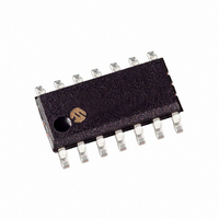
PIC16F616-I/SL Microchip Technology, PIC16F616-I/SL Datasheet - Page 60

PIC16F616-I/SL
Manufacturer Part Number
PIC16F616-I/SL
Description
IC PIC MCU FLASH 2KX14 14SOIC
Manufacturer
Microchip Technology
Series
PIC® 16Fr
Datasheets
1.PIC12F609T-ISN.pdf
(26 pages)
2.PIC16F616T-ISL.pdf
(4 pages)
3.PIC16F616T-ISL.pdf
(214 pages)
4.PIC16F616T-ISL.pdf
(8 pages)
5.PIC16F616-ESL.pdf
(180 pages)
Specifications of PIC16F616-I/SL
Program Memory Type
FLASH
Program Memory Size
3.5KB (2K x 14)
Package / Case
14-SOIC (3.9mm Width), 14-SOL
Core Processor
PIC
Core Size
8-Bit
Speed
20MHz
Peripherals
Brown-out Detect/Reset, POR, PWM, WDT
Number Of I /o
11
Ram Size
128 x 8
Voltage - Supply (vcc/vdd)
2 V ~ 5.5 V
Data Converters
A/D 8x10b
Oscillator Type
Internal
Operating Temperature
-40°C ~ 85°C
Processor Series
PIC16F
Core
PIC
Data Bus Width
8 bit
Data Ram Size
128 B
Maximum Clock Frequency
20 MHz
Number Of Programmable I/os
11
Number Of Timers
3
Maximum Operating Temperature
+ 85 C
Mounting Style
SMD/SMT
3rd Party Development Tools
52715-96, 52716-328, 52717-734
Development Tools By Supplier
PG164130, DV164035, DV244005, DV164005, PG164120, ICE2000
Minimum Operating Temperature
- 40 C
On-chip Adc
10 bit, 8 Channel
Lead Free Status / RoHS Status
Lead free / RoHS Compliant
For Use With
MCP1631RD-DCPC1 - REF DES BATT CHARG OR LED DRIVERAC162083 - HEADER MPLAB ICD2 PIC16F616 8/14
Eeprom Size
-
Connectivity
-
Lead Free Status / Rohs Status
Lead free / RoHS Compliant
Available stocks
Company
Part Number
Manufacturer
Quantity
Price
Company:
Part Number:
PIC16F616-I/SL
Manufacturer:
MICROCHIP
Quantity:
400
Company:
Part Number:
PIC16F616-I/SL
Manufacturer:
Microchip Technology
Quantity:
45 197
Part Number:
PIC16F616-I/SL
Manufacturer:
MICROCHIP
Quantity:
20 000
PIC16F610/616/16HV610/616
8.4
The comparator interrupt flag can be set whenever
there is a change in the output value of the comparator.
Changes are recognized by means of a mismatch
circuit which consists of two latches and an
exclusive-or gate (see Figure 8-2 and Figure 8-3). One
latch is updated with the comparator output level when
the CMxCON0 register is read. This latch retains the
value until the next read of the CMxCON0 register or
the occurrence of a Reset. The other latch of the
mismatch circuit is updated on every Q1 system clock.
A mismatch condition will occur when a comparator
output change is clocked through the second latch on
the Q1 clock cycle. At this point the two mismatch
latches have opposite output levels which is detected
by the exclusive-or gate and fed to the interrupt
circuitry. The mismatch condition persists until either
the CMxCON0 register is read or the comparator
output returns to the previous state.
The comparator interrupt is set by the mismatch edge
and not the mismatch level. This means that the inter-
rupt flag can be reset without the additional step of
reading or writing the CMxCON0 register to clear the
mismatch registers. When the mismatch registers are
cleared, an interrupt will occur upon the comparator’s
return to the previous state, otherwise no interrupt will
be generated.
Software will need to maintain information about the
status of the comparator output, as read from the
CMxCON0 register, or CM2CON1 register, to determine
the actual change that has occurred.
The CxIF bit of the PIR1 register is the comparator
interrupt flag. This bit must be reset in software by
clearing it to ‘0’. Since it is also possible to write a ‘1’ to
this register, an interrupt can be generated.
The CxIE bit of the PIE1 register and the PEIE and GIE
bits of the INTCON register must all be set to enable
comparator interrupts. If any of these bits are cleared,
the interrupt is not enabled, although the CxIF bit of the
PIR1 register will still be set if an interrupt condition
occurs.
DS41288F-page 60
Note 1: A write operation to the CMxCON0
2: Comparator interrupts will operate correctly
Comparator Interrupt Operation
register will also clear the mismatch
condition because all writes include a read
operation at the beginning of the write
cycle.
regardless of the state of CxOE.
FIGURE 8-4:
FIGURE 8-5:
Q1
Q3
CxIN+
CxOUT
Set CxIF (edge)
CxIF
Q1
Q3
CxIN+
CxOUT
Set CxIF (edge)
CxIF
Note 1: If a change in the CMxCON0 register
cleared by CMxCON0 read
2: When either comparator is first enabled,
(CxOUT) should occur when a read oper-
ation is being executed (start of the Q2
cycle), then the CxIF of the PIR1 register
interrupt flag may not get set.
bias circuitry in the comparator module
may cause an invalid output from the
comparator until the bias circuitry is stable.
Allow about 1 μs for bias settling then clear
the mismatch condition and interrupt flags
before enabling comparator interrupts.
T
T
RT
RT
COMPARATOR
INTERRUPT TIMING W/O
CMxCON0 READ
COMPARATOR
INTERRUPT TIMING WITH
CMxCON0 READ
© 2009 Microchip Technology Inc.
reset by software
reset by software


