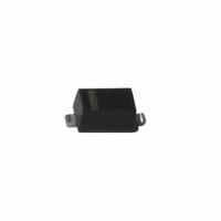
PESD5V0S1BB,115 NXP Semiconductors, PESD5V0S1BB,115 Datasheet - Page 8

PESD5V0S1BB,115
Manufacturer Part Number
PESD5V0S1BB,115
Description
DIODE BIDIR ESD PROTECT SOD523
Manufacturer
NXP Semiconductors
Datasheet
1.PESD5V0S1BA115.pdf
(15 pages)
Specifications of PESD5V0S1BB,115
Package / Case
SC-79, SOD-523
Voltage - Reverse Standoff (typ)
5V
Voltage - Breakdown
5.5V
Power (watts)
130W
Polarization
Bidirectional
Mounting Type
Surface Mount
Polarity
Bidirectional
Clamping Voltage
14 V
Operating Voltage
5 V
Breakdown Voltage
9.5 V
Termination Style
SMD/SMT
Peak Surge Current
12 A
Peak Pulse Power Dissipation
130 W
Capacitance
35 pF
Maximum Operating Temperature
+ 150 C
Minimum Operating Temperature
- 65 C
Dimensions
0.85(Max) mm W x 1.25(Max) mm L
Lead Free Status / RoHS Status
Lead free / RoHS Compliant
Lead Free Status / RoHS Status
Lead free / RoHS Compliant, Lead free / RoHS Compliant
Other names
568-4054-2
934058005115
PESD5V0S1BB T/R
PESD5V0S1BB T/R
934058005115
PESD5V0S1BB T/R
PESD5V0S1BB T/R
Available stocks
Company
Part Number
Manufacturer
Quantity
Price
Company:
Part Number:
PESD5V0S1BB,115
Manufacturer:
NXP Semiconductors
Quantity:
7 200
Part Number:
PESD5V0S1BB,115
Manufacturer:
NEXPERIA/安世
Quantity:
20 000
NXP Semiconductors
7. Application information
PESD5V0S1BA_BB_BL_4
Product data sheet
PESD5V0S1Bx series is designed for the protection of one bidirectional signal line from
the damage caused by ElectroStatic Discharge (ESD) and surge pulses. The devices may
be used on lines where the signal polarities are above and below ground. They provide a
surge capability of up to 130 W per line for a 8/20 s waveform.
Circuit board layout and protection device placement:
Circuit board layout is critical for the suppression of ESD, EFT and surge transients.
The following guidelines are recommended:
1. Place the protection device as close to the input terminal or connector as possible.
2. The path length between the protection device and the protected line should be
3. Keep parallel signal paths to a minimum.
4. Avoid running protection conductors in parallel with unprotected conductor.
5. Minimize all printed-circuit board conductive loops including power and ground loops.
6. Minimize the length of the transient return path to ground.
7. Avoid using shared transient return paths to a common ground point.
8. Ground planes should be used whenever possible. For multilayer printed-circuit
Fig 8.
minimized.
boards, use ground vias.
Bidirectional protection of one signal line
Rev. 04 — 20 August 2009
signal line
Low capacitance bidirectional ESD protection diodes
PESD5V0S1BA/BB/BL
PESD5V0S1Bx
006aaa057
GND
© NXP B.V. 2009. All rights reserved.
8 of 15


