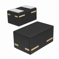
PESD5V0X1BL,315 NXP Semiconductors, PESD5V0X1BL,315 Datasheet - Page 6

PESD5V0X1BL,315
Manufacturer Part Number
PESD5V0X1BL,315
Description
DIODE ESD PROT BI-DIR 5V SOD-882
Manufacturer
NXP Semiconductors
Specifications of PESD5V0X1BL,315
Package / Case
SOD-882
Voltage - Reverse Standoff (typ)
5V
Voltage - Breakdown
7.5V
Polarization
Bidirectional
Mounting Type
Surface Mount
Polarity
Bidirectional
Channels
1 Channel
Operating Voltage
5 V
Breakdown Voltage
7.5 V
Termination Style
SMD/SMT
Capacitance
0.9 pF
Maximum Operating Temperature
+ 150 C
Minimum Operating Temperature
- 55 C
Dimensions
1.35 mm W x 2.7 mm L x 1.1 mm H
Number Of Elements
1
Package Type
SOD-882
Operating Temperature Classification
Military
Reverse Breakdown Voltage
6V
Reverse Stand-off Voltage
5V
Leakage Current (max)
100nA
Test Current (it)
5mA
Operating Temp Range
-55C to 150C
Mounting
Surface Mount
Pin Count
2
Lead Free Status / RoHS Status
Lead free / RoHS Compliant
Power (watts)
-
Lead Free Status / Rohs Status
Lead free / RoHS Compliant
Other names
568-4674-2
934061649315
PESD5V0X1BL T/R
934061649315
PESD5V0X1BL T/R
NXP Semiconductors
7. Application information
8. Test information
PESD5V0X1BL_2
Product data sheet
8.1 Quality information
PESD5V0X1BL is designed for the protection of one bidirectional data or signal line from
the damage caused by ESD. The device may be used on lines where the signal polarities
are both, positive and negative with respect to ground.
Circuit board layout and protection device placement
Circuit board layout is critical for the suppression of ESD and Electrical Fast
Transient (EFT). The following guidelines are recommended:
This product has been qualified in accordance with the Automotive Electronics Council
(AEC) standard Q101 - Stress test qualification for discrete semiconductors , and is
suitable for use in automotive applications.
1. Place the device as close to the input terminal or connector as possible.
2. The path length between the device and the protected line should be minimized.
3. Keep parallel signal paths to a minimum.
4. Avoid running protected conductors in parallel with unprotected conductors.
5. Minimize all Printed-Circuit Board (PCB) conductive loops including power and
6. Minimize the length of the transient return path to ground.
7. Avoid using shared transient return paths to a common ground point.
8. Ground planes should be used whenever possible. For multilayer PCBs, use ground
Fig 5.
ground loops.
vias.
Application diagram
Rev. 02 — 16 July 2009
Ultra low capacitance bidirectional ESD protection diode
line to be protected
PESD5V0X1BL
GND
006aab250
PESD5V0X1BL
© NXP B.V. 2009. All rights reserved.
6 of 11


