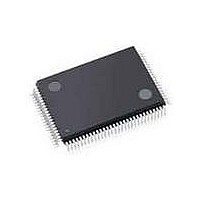
C8051F040-TB Silicon Laboratories Inc, C8051F040-TB Datasheet - Page 71

C8051F040-TB
Manufacturer Part Number
C8051F040-TB
Description
BOARD PROTOTYPING W/C8051F040
Manufacturer
Silicon Laboratories Inc
Type
MCUr
Specifications of C8051F040-TB
Contents
Board
Processor To Be Evaluated
C8051F04x
Interface Type
USB
Lead Free Status / RoHS Status
Contains lead / RoHS non-compliant
For Use With/related Products
C8051F040
Lead Free Status / Rohs Status
Lead free / RoHS Compliant
- Current page: 71 of 328
- Download datasheet (3Mb)
Bits7-4:
Bit3:
Bit2:
Bit1:
Bit0:
NOTE:
Bits7-4:
Bits3-0:
Bit7
Bit7
R
R
-
-
UNUSED. Read = 0000b; Write = don’t care
PORT3IC: Port 3 even/odd Pin Input Pair Configuration Bit
0: Port 3 even and odd input channels are independent single-ended inputs
1: Port 3 even and odd input channels are (respectively) +, - differential input pair
HVDA2C: HVDA 2’s Compliment Bit
0: HVDA output measured as an independent single-ended input
1: 2’s compliment value Result from HVDA
AIN23IC: AIN2, AIN3 Input Pair Configuration Bit
0: AIN2 and AIN3 are independent single-ended inputs
1: AIN2, AIN3 are (respectively) +, - differential input pair
AIN01IC: AIN0, AIN1 Input Pair Configuration Bit
0: AIN0 and AIN1 are independent single-ended inputs
1: AIN0, AIN1 are (respectively) +, - differential input pair
The ADC0 Data Word is in 2’s complement format for channels configured as differential.
UNUSED. Read = 0000b; Write = don’t care
AMX0AD3-0: AMX0 Address Bits
0000-1111b: ADC Inputs selected per Table 6.1.
Bit6
Bit6
R
R
-
-
SFR Definition 6.2. AMX0SL: AMUX0 Channel Select
SFR Definition 6.1. AMX0CF: AMUX0 Configuration
Bit5
Bit5
R
R
-
-
Bit4
Bit4
R
R
-
-
AMX0AD3 AMX0AD2 AMX0AD1 AMX0AD0 00000000
PORT3IC HVDA2C
Rev. 1.5
R/W
R/W
Bit3
Bit3
C8051F040/1/2/3/4/5/6/7
R/W
R/W
Bit2
Bit2
AIN23IC
R/W
R/W
Bit1
Bit1
SFR Address:
SFR Address:
AIN01IC
SFR Page:
SFR Page:
R/W
R/W
Bit0
Bit0
0xBA
0
0xBB
0
SFR Address:
Reset Value
00000000
Reset Value
71
Related parts for C8051F040-TB
Image
Part Number
Description
Manufacturer
Datasheet
Request
R
Part Number:
Description:
SMD/C°/SINGLE-ENDED OUTPUT SILICON OSCILLATOR
Manufacturer:
Silicon Laboratories Inc
Part Number:
Description:
Manufacturer:
Silicon Laboratories Inc
Datasheet:
Part Number:
Description:
N/A N/A/SI4010 AES KEYFOB DEMO WITH LCD RX
Manufacturer:
Silicon Laboratories Inc
Datasheet:
Part Number:
Description:
N/A N/A/SI4010 SIMPLIFIED KEY FOB DEMO WITH LED RX
Manufacturer:
Silicon Laboratories Inc
Datasheet:
Part Number:
Description:
N/A/-40 TO 85 OC/EZLINK MODULE; F930/4432 HIGH BAND (REV E/B1)
Manufacturer:
Silicon Laboratories Inc
Part Number:
Description:
EZLink Module; F930/4432 Low Band (rev e/B1)
Manufacturer:
Silicon Laboratories Inc
Part Number:
Description:
I°/4460 10 DBM RADIO TEST CARD 434 MHZ
Manufacturer:
Silicon Laboratories Inc
Part Number:
Description:
I°/4461 14 DBM RADIO TEST CARD 868 MHZ
Manufacturer:
Silicon Laboratories Inc
Part Number:
Description:
I°/4463 20 DBM RFSWITCH RADIO TEST CARD 460 MHZ
Manufacturer:
Silicon Laboratories Inc
Part Number:
Description:
I°/4463 20 DBM RADIO TEST CARD 868 MHZ
Manufacturer:
Silicon Laboratories Inc
Part Number:
Description:
I°/4463 27 DBM RADIO TEST CARD 868 MHZ
Manufacturer:
Silicon Laboratories Inc
Part Number:
Description:
I°/4463 SKYWORKS 30 DBM RADIO TEST CARD 915 MHZ
Manufacturer:
Silicon Laboratories Inc
Part Number:
Description:
N/A N/A/-40 TO 85 OC/4463 RFMD 30 DBM RADIO TEST CARD 915 MHZ
Manufacturer:
Silicon Laboratories Inc
Part Number:
Description:
I°/4463 20 DBM RADIO TEST CARD 169 MHZ
Manufacturer:
Silicon Laboratories Inc


