MPC8349E-MITXE Freescale Semiconductor, MPC8349E-MITXE Datasheet - Page 37
MPC8349E-MITXE
Manufacturer Part Number
MPC8349E-MITXE
Description
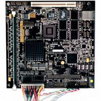
BOARD REFERENCE FOR MPC8349
Manufacturer
Freescale Semiconductor
Series
PowerQUICC II™ PROr
Type
MPUr
Specifications of MPC8349E-MITXE
Contents
Module and Misc Hardware
Processor To Be Evaluated
MPC8349E
Interface Type
Ethernet, USB
Silicon Manufacturer
Freescale
Core Architecture
Power Architecture
Core Sub-architecture
PowerQUICC
Silicon Core Number
MPC83xx
Silicon Family Name
PowerQUICC II PRO
Rohs Compliant
Yes
For Use With/related Products
MPC8349E
Lead Free Status / RoHS Status
Lead free / RoHS Compliant
Other names
MPC8349E-MITXE


1.6.5
The MPC8349E requires a 3.3 V and 5 V power supply from the ATX power connector for normal
operation. The 3.3 V power supply is reduced to 1.2 V and 2.5 V. The 1.2 V power is generated from a
switching power supply for a CPU core and the GBE L2 switch. The 2.5 V power is generated from an
LDO regulator for the DDR controller.
Figure 27
The core supply voltage and I/O supply voltages do not have to be applied in any particular order. During
the power ramp up, before the power supplies are stable, there may be an interval when the I/O pins are
actively driven. After power is stable, as long as PORESET is asserted, most I/O pins are three-stated. To
minimize the time I/O pins are actively driven, apply core voltage before I/O voltage and assert PORESET
before the power supplies fully ramp up. In general, for a dual-supply voltage device, minimize the voltage
difference between the V
1.6.6
Table 23
memory.
Freescale Semiconductor
0x0000_0000–0x4000_0000
0x8000_0000–0x9FFF_FFFF
0xE200_0000–0xE2FF_FFFF
0xA000_0000–0xBFFF_FFFF
5 V input
3.3 V input
Address Range
shows an example memory map on the MPC8349E that is used for u-boot 1.1.3 in the Flash
Table 23. Example Memory Map, Local Access Window, and Chip-Select Assignments
shows the power supply block diagram.
Power Supply
Chip-Select Assignments and Memory Map
MPC8349E-mITXE Reference Design Platform User’s Guide, Rev. 2
CPU Fan
core
5 V
Target Interface
and V
Preliminary—Subject to Change Without Notice
DDR
PCI1
PCI1
PCI2
I/O
Figure 27. Power Supply Circuitry
during ramp-up and power-down.
MCS0/MCS1
Chip-Select
Line
Nil
Nil
Nil
MAX1953
MIC2505
MIC29302
DDR SDRAM (256 Mbytes– 1
Gbyte)
PCI1 memory space (512 Mbyte)
PCI1 I/O space (16 Mbyte)
PCI2 memory space (512 Mbyte)
Device Name
MPC8349E Vcore, VSC7385
USB VBUS Power
1.2 V
5 V
3.3 V
DDR
2.5 V
MPC8349E-mITXE Board
Port Size (Bits)
64
32
32
32
37
Related parts for MPC8349E-MITXE
Image
Part Number
Description
Manufacturer
Datasheet
Request
R

Part Number:
Description:
KIT REFERENCE PLATFORM MPC8349E
Manufacturer:
Freescale Semiconductor
Datasheet:
Part Number:
Description:
KIT MODULAR DEV SYSTEM MPC8349E
Manufacturer:
Freescale Semiconductor
Datasheet:

Part Number:
Description:
MCU, MPU & DSP Development Tools PROCESSR BD MPC8349E
Manufacturer:
Freescale Semiconductor
Part Number:
Description:
MCU, MPU & DSP Development Tools KIT FOR MPC8349E BDS
Manufacturer:
Freescale Semiconductor

Part Number:
Description:
Manufacturer:
Freescale Semiconductor, Inc
Datasheet:
Part Number:
Description:
Manufacturer:
Freescale Semiconductor, Inc
Datasheet:
Part Number:
Description:
Manufacturer:
Freescale Semiconductor, Inc
Datasheet:
Part Number:
Description:
Manufacturer:
Freescale Semiconductor, Inc
Datasheet:
Part Number:
Description:
Manufacturer:
Freescale Semiconductor, Inc
Datasheet:
Part Number:
Description:
Manufacturer:
Freescale Semiconductor, Inc
Datasheet:
Part Number:
Description:
Manufacturer:
Freescale Semiconductor, Inc
Datasheet:
Part Number:
Description:
Manufacturer:
Freescale Semiconductor, Inc
Datasheet:
Part Number:
Description:
Manufacturer:
Freescale Semiconductor, Inc
Datasheet:
Part Number:
Description:
Manufacturer:
Freescale Semiconductor, Inc
Datasheet:
Part Number:
Description:
Manufacturer:
Freescale Semiconductor, Inc
Datasheet: