MPC8349E-MITXE Freescale Semiconductor, MPC8349E-MITXE Datasheet - Page 31
MPC8349E-MITXE
Manufacturer Part Number
MPC8349E-MITXE
Description
BOARD REFERENCE FOR MPC8349
Manufacturer
Freescale Semiconductor
Series
PowerQUICC II™ PROr
Type
MPUr
Specifications of MPC8349E-MITXE
Contents
Module and Misc Hardware
Processor To Be Evaluated
MPC8349E
Interface Type
Ethernet, USB
Silicon Manufacturer
Freescale
Core Architecture
Power Architecture
Core Sub-architecture
PowerQUICC
Silicon Core Number
MPC83xx
Silicon Family Name
PowerQUICC II PRO
Rohs Compliant
Yes
For Use With/related Products
MPC8349E
Lead Free Status / RoHS Status
Lead free / RoHS Compliant
Other names
MPC8349E-MITXE


The two Flash memory banks are MX29LV640MTTC-90 top boot Flash memory devices. Each Flash
memory bank has 135 sectors. The first 127 sectors, SA[0–126], are 64 Kbyte, and the last 8 sectors,
SA[127–134], are 8 Kbyte. These last 8 sectors can be write-protected to prevent accidental erasure of the
sector content for applications that may choose to use this protection feature.
settings to write-protect sectors SA[127–134] of Flash memory.
1.6.2
An on-board serial EEPROM allows storage of miscellaneous board-related data. The EEPROM can be
write-protected by S2.SW3, as shown in
1.6.3
An M66EN input pin determines the AC timing of the PCI interface. On the MPC8349E-mITXE board,
the state of this signal can be driven to 0 by the J22 jumper to select 33 MHz AC timing. If J22.F is not
driven to 0, the M66EN signal level is determined by the PCI agent card connected to PCI slot P1. If a 33
MHz only card is inserted, the M66EN signal is driven to 0 by the PCI agent card according to the PCI
specification, or it is driven to 1 if it can perform at 66 MHz. See
Freescale Semiconductor
.
Jumper Off
Jumper On
J22.F
EEPROM
PCI Operating Frequency
Jumper Off
Jumper On
M66EN signal is determined by the card plugged into the PCI slot (PCI 32-bit slot and MiniPCI slot).
M66EN signal is hardwired to 0, which is hard coded to 33 MHz PCI operation.
J22.H
Jumper Off
Jumper On
Jumper Off
Jumper On
J22.E
J22.G
MPC8349E-mITXE Reference Design Platform User’s Guide, Rev. 2
Table 16. Flash Memory Write Protect of SA[127–134]
Flash (U4 and U7) top sectors are not write protected (WP not asserted).
Flash (U4 and U7) top sectors are write protected (WP asserted).
Table 15. Flash Bank for Booting the System
Table 18. M66EN Signal Status Selection
Serial EEPROM is write protected (WC not asserted).
Serial EEPROM is not write protected (WC asserted).
The booting bank is U4.
The booting bank is U7.
Preliminary—Subject to Change Without Notice
Table 17. EEPROM Write Protect
Table
17.
Description
Description
Description
Description
Table
18.
Table 16
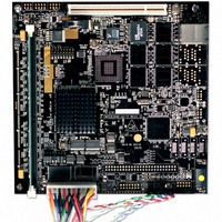
MPC8349E-mITXE Board
shows the jumper
31
Related parts for MPC8349E-MITXE
Image
Part Number
Description
Manufacturer
Datasheet
Request
R

Part Number:
Description:
KIT REFERENCE PLATFORM MPC8349E
Manufacturer:
Freescale Semiconductor
Datasheet:
Part Number:
Description:
KIT MODULAR DEV SYSTEM MPC8349E
Manufacturer:
Freescale Semiconductor
Datasheet:

Part Number:
Description:
MCU, MPU & DSP Development Tools PROCESSR BD MPC8349E
Manufacturer:
Freescale Semiconductor
Part Number:
Description:
MCU, MPU & DSP Development Tools KIT FOR MPC8349E BDS
Manufacturer:
Freescale Semiconductor

Part Number:
Description:
Manufacturer:
Freescale Semiconductor, Inc
Datasheet:
Part Number:
Description:
Manufacturer:
Freescale Semiconductor, Inc
Datasheet:
Part Number:
Description:
Manufacturer:
Freescale Semiconductor, Inc
Datasheet:
Part Number:
Description:
Manufacturer:
Freescale Semiconductor, Inc
Datasheet:
Part Number:
Description:
Manufacturer:
Freescale Semiconductor, Inc
Datasheet:
Part Number:
Description:
Manufacturer:
Freescale Semiconductor, Inc
Datasheet:
Part Number:
Description:
Manufacturer:
Freescale Semiconductor, Inc
Datasheet:
Part Number:
Description:
Manufacturer:
Freescale Semiconductor, Inc
Datasheet:
Part Number:
Description:
Manufacturer:
Freescale Semiconductor, Inc
Datasheet:
Part Number:
Description:
Manufacturer:
Freescale Semiconductor, Inc
Datasheet:
Part Number:
Description:
Manufacturer:
Freescale Semiconductor, Inc
Datasheet: