STEVAL-ISA026V1 STMicroelectronics, STEVAL-ISA026V1 Datasheet
STEVAL-ISA026V1
Specifications of STEVAL-ISA026V1
Available stocks


Related parts for STEVAL-ISA026V1


STEVAL-ISA026V1 Summary of contents
Page 1
Adjustable step-down controller with synchronous rectification Features ■ Input voltage range from 1 ■ Supply voltage range from 4 ■ Adjustable output voltage down to 0.6 V with ± 0.8 % accuracy ...
Page 2
Contents Contents 1 Summary description . . . . . . . . . . . . . . . . . . . . . . . . . . . . . . . . . . . ...
Page 3
L6732 7 board description and PCB layout . . . . . . . . . . . . . . . . . . . . . . . . . . 26 7 board ...
Page 4
Summary description 1 Summary description The controller is an integrated circuit realized in BCD5 (BiCMOS-DMOS, version 5) fabrication that provides complete control logic and protection for high performance step- down DC-DC and niPoL converters designed to drive N-channel ...
Page 5
L6732 1.1 Functional description Figure 1. Block diagram SS SS EAREF EAREF PGOOD SYNCH Vcc=4.5V-14V OCH OCH OCL OCL VCCDR VCCDR LDO LDO Monitor Monitor Protection and Ref Protection and Ref OSC OSC - - L6732 - - + + ...
Page 6
Electrical data 2 Electrical data 2.1 Maximum rating Table 2. Absolute maximum ratings Symbol BOOT - Boot voltage V PHASE V HGATE - V PHASE V BOOT BOOT PHASE V PHASE PHASE spike, transient < ...
Page 7
L6732 3 Pin connection and function Figure 2. Pin connection (top view) Table 4. Pin functions Pin n. Name 1 PGOOD 2 SYNCH 3 SGND COMP 6 SS/INH PGOOD 16 1 SYNCH 15 2 SGND 14 3 ...
Page 8
Pin connection and function Table 4. Pin functions (continued) Pin n. Name 7 EAREF 8 OCL 9 OCH 10 PHASE 11 HGATE 12 BOOT 13 PGND 14 LGATE 15 V CCDR 8/37 Function By setting the voltage ...
Page 9
L6732 4 Electrical characteristics Table 5. Electrical characteristics ( °C, unless otherwise specified Symbol Parameter V supply current CC V stand by current quiescent current CC Power-ON V ...
Page 10
Electrical characteristics Table 5. Electrical characteristics ( °C, unless otherwise specified) (continued Symbol Parameter Gate drivers R High side source resistance HGATE_ON R High side sink resistance HGATE_OFF R Low side source ...
Page 11
L6732 5 Device description 5.1 Oscillator The switching frequency can be fixed to two values: 250 kHz or 500 kHz by setting the proper voltage at the EAREF pin (see external reference). 5.2 Internal LDO An internal LDO supplies the ...
Page 12
Device description 5.3 Bypassing the LDO to avoid the voltage drop with low Vcc ≈ the internal LDO works in dropout with an output resistance of about 1 Ω. The maximum LDO output current is ...
Page 13
L6732 5.5 Error amplifier Figure 5. Error amplifier reference 5.6 Soft-start When both V and V CC pin) the start-up phase takes place. Otherwise the SS pin is internally shorted to GND. At start-up, a ramp is generated charging the ...
Page 14
Device description Figure 6. Device start-up: voltage at the SS pin Vss Figure 7. Start-up without pre-bias 14/37 Vcc Vin 4.2V 1.25V 4V 0.5V L6732 LGate V OUT ...
Page 15
L6732 Figure 8. Start-up with pre-bias The L6732 can sink or source current after the soft-start phase (see current is detected during the soft-start phase, the device provides a constant-current- protection. In this way, in case of short soft-start time ...
Page 16
Device description 5.7 Driver section The high-side and low-side drivers allow using different types of power MOSFETs (also multiple MOSFETs to reduce the R The low-side driver is supplied by V pin. A predictive dead time control avoids MOSFETs cross-conduction ...
Page 17
L6732 rises with a slope of 100 mV/µs, emulating in this way the breaking of the high-side MOSFET as an over-voltage cause. Figure 11. OVP: the low-side MOSFET is turned-on in advance The device realizes the over-current-protection (OCP) sensing the ...
Page 18
Device description Equation 4 During soft-start the OC acts in constant current mode: a current control loop limits the value of the error amplifier output (comp), in order to avoid its saturation and thus recover faster when the output returns ...
Page 19
L6732 other one will be the slave. The Slave controller will increase its switching frequency reducing the ramp amplitude proportionally and then the modulator gain will be increased. Figure 13. Synchronization: PWM signal Figure 14. Synchronization: Inductor currents To avoid ...
Page 20
Device description 5.11 Minimum on-time (T The device can manage minimum on-times lower than 100 ns. This feature comes down from the control topology and from the particular over-current-protection system of the L6732. In fact voltage mode controller ...
Page 21
L6732 5.12 Bootstrap anti-discharging system This built-in system avoids that the voltage across the bootstrap capacitor becomes less than 3 internal comparator senses the voltage across the external bootstrap capacitor keeping it charged, eventually turning-on the low-side MOSFET ...
Page 22
Application details 6 Application details 6.1 Inductor design The inductance value is defined by a compromise between the transient response time, the efficiency, the cost and the size. The inductor has to be calculated to sustain the output and the ...
Page 23
L6732 6.2 Output capacitors The output capacitors are basic components for the fast transient response of the power supply. They depend on the output voltage ripple requirements, as well as any output voltage deviation requirement during a load transient. During ...
Page 24
Application details Where D is the duty cycle. The equation reaches its maximum value, I The losses in worst case are: Equation 12 6.4 Compensation network The loop is based on a voltage mode control the internal/external reference voltage and ...
Page 25
L6732 Equation 14 ● Compensation network singularity frequencies: Equation 15 Equation 16 Equation 17 Equation 18 ● Compensation network design: – Equation 19 – – – – – ω = ESR ESR 1 ω ⎛ C ⎜ ...
Page 26
Application details Figure 19. Asymptotic bode plot of converter's open loop gain 26/37 L6732 ...
Page 27
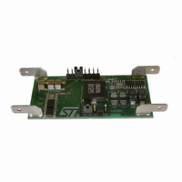
L6732 7 L6732 demonstration board 7 board description and PCB layout L6732 20 A demonstration board realizes in a four layer PCB a step-down DC/DC converter and shows the operation of the device in a general purpose application. ...
Page 28
L6732 demonstration board Table 7. Demonstration board part list Reference R10 R11 R12 R13 C10 C11 C12-13 C15 C16- ...
Page 29
L6732 Table 8. Other inductor manufacturer Manufacturer Wurth elektronic SUMIDA EPCOS TDK TOKO COILTRONICS Table 9. Other capacitor manufacturer Manufacturer TDK NIPPON CHEMI-CON PANASONIC Figure 21. Demonstration board efficiency ...
Page 30
L6732 demonstration board Figure 22. Top layer Figure 23. Power ground layer Figure 24. Signal-ground layer Figure 25. Bottom layer 30/37 L6732 ...
Page 31
L6732 7 board description and PCB layout L6732 5 A demonstration board realizes in a two layer PCB a step-down DC/DC converter and shows the operation of the device in a general purpose application. The input voltage can ...
Page 32
L6732 demonstration board Table 10. Demonstration board part list (continued) Reference C12-13 C15 C16- Figure 26. Demonstration board efficiency 32/37 Value Manufacturer 3X 10 µ 330 µF / 2,7 µH Coilcraft ...
Page 33
L6732 Figure 27. Top layer Figure 28. Power ground layer L6732 demonstration board 33/37 ...
Page 34
Package mechanical data 8 Package mechanical data In order to meet environmental requirements, ST offers these devices in ECOPACK packages. These packages have a lead-free second level interconnect. The category of second Level Interconnect is marked on the package and ...
Page 35
L6732 Figure 29. HTSSOP16 mechanical data DIM TSSOP16 EXPOSED PAD MECHANICAL DATA mm. MIN. TYP MAX. 1.2 0.15 0.8 1 1.05 0.19 0.30 0.09 0.20 4.9 5 ...
Page 36
Revision history 9 Revision history Table 11. Document revision history Date 20-Dec-2005 24-Jan-2006 29-May-2006 26-Jun-2006 25-Sep-2006 04-Jun-2008 36/37 Revision 1 Initial release 2 Improved description of soft-start, in case of pre-bias start-up 3 New template, thermal data updated 4 Note ...
Page 37
... L6732 Information in this document is provided solely in connection with ST products. STMicroelectronics NV and its subsidiaries (“ST”) reserve the right to make changes, corrections, modifications or improvements, to this document, and the products and services described herein at any time, without notice. All ST products are sold pursuant to ST’s terms and conditions of sale. ...