AD9516-4/PCBZ Analog Devices Inc, AD9516-4/PCBZ Datasheet - Page 6
AD9516-4/PCBZ
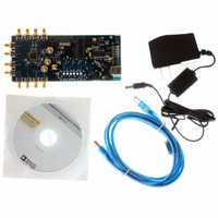
Manufacturer Part Number
AD9516-4/PCBZ
Description
BOARD EVAL FOR AD9516-4 1.8GHZ
Manufacturer
Analog Devices Inc
Specifications of AD9516-4/PCBZ
Main Purpose
Timing, Clock Generator
Embedded
No
Utilized Ic / Part
AD9516-4
Primary Attributes
2 Inputs, 14 Outputs, 1.6GHz VCO
Secondary Attributes
CMOS, LVDS, LVPECL Output Logic, ADIsimCLK™ Graphical User Interface
Silicon Manufacturer
Analog Devices
Application Sub Type
PLL Clock Synthesizer
Kit Application Type
Clock & Timing
Silicon Core Number
AD9516-0, AD9516-1, AD9516-2
Silicon Family Name
AD9516-X
Rohs Compliant
Yes
Lead Free Status / RoHS Status
Lead free / RoHS Compliant


AD9516-4
CLOCK INPUTS
Table 3.
Parameter
CLOCK INPUTS (CLK, CLK)
1
CLOCK OUTPUTS
Table 4.
Parameter
LVPECL CLOCK OUTPUTS
LVDS CLOCK OUTPUTS
CMOS CLOCK OUTPUTS
Below about 1 MHz, the input should be dc-coupled. Care should be taken to match V
OUT6, OUT7, OUT8, OUT9
OUT0, OUT1, OUT2, OUT3, OUT4, OUT5
Input Frequency
Input Sensitivity, Differential
Input Common-Mode Range, V
Input Sensitivity, Single-Ended
Input Resistance
Input Capacitance
OUT6A, OUT6B, OUT7A, OUT7B,
Input Level, Differential
Input Common-Mode Voltage, V
Output Frequency, Maximum
Output High Voltage (V
Output Low Voltage (V
Output Differential Voltage (V
Output Frequency
Differential Output Voltage (V
Delta V
Output Offset Voltage (V
Delta V
Short-Circuit Current (I
OUT8A, OUT8B, OUT9A, OUT9B
Output Frequency
Output Voltage High (V
Output Voltage Low (V
OD
OS
SA
OL
OH
, I
)
OL
OS
OH
)
SB
)
)
)
)
OD
OD
CMR
CM
)
)
Min
0
0
1.3
1.3
3.9
Min
2950
V
V
550
247
1.125
V
1
S
S
S
1
− 1.12
− 2.03
− 0.1
Typ
150
1.57
150
4.7
2
Typ
V
V
790
360
1.24
14
S
S
− 0.98
− 1.77
Rev. A | Page 6 of 80
Max
2.4
1.6
2
1.8
1.8
5.7
Max
V
V
980
800
454
25
1.375
25
24
250
0.1
S
S
− 0.84
− 1.49
CM
.
Unit
GHz
V
Unit
mA
GHz
mV p-p
V p-p
V
mV p-p
kΩ
pF
MHz
V
V
mV
MHz
mV
mV
V
mV
MHz
V
V
Test Conditions/Comments
Differential input
High frequency distribution (VCO divider)
Distribution only (VCO divider bypassed)
Measured at 2.4 GHz; jitter performance is improved
with slew rates > 1 V/ns
Larger voltage swings may turn on the protection
diodes and may degrade jitter performance
Self-biased; enables ac coupling
With 200 mV p-p signal applied; dc-coupled
CLK ac-coupled; CLK ac-bypassed to RF ground
Self-biased
Test Conditions/Comments
Termination = 50 Ω to V
Differential (OUT, OUT)
Using direct to output; see Figure 25 for peak-to –
peak differential amplitude
V
amplitude setting with driver not toggling; see
Figure 25 for variation over frequency
Differential termination 100 Ω at 3.5 mA
Differential (OUT, OUT)
The AD9516 outputs toggle at higher frequencies,
but the output amplitude may not meet the V
specification; see Figure 26
V
the default amplitude setting with output driver
not toggling; see Figure 26 for variation over
frequency
This is the absolute value of the difference
between V
when the complementary output is high
(V
This is the absolute value of the difference
between V
when the complementary output is high
Output shorted to GND
Single-ended; termination = 10 pF
See Figure 27
At 1 mA load
At 1 mA load
OH
OH
OH
− V
− V
+ V
OL
OL
OL
for each leg of a differential pair for default
measurement across a differential pair at
)/2 across a differential pair
OD
OS
when the normal output is high vs.
when the normal output is high vs.
S
− 2 V
OD
Related parts for AD9516-4/PCBZ
Image
Part Number
Description
Manufacturer
Datasheet
Request
R

Part Number:
Description:
IC CLOCK PLL/VCO 2GHZ 64LFCSP
Manufacturer:
Analog Devices Inc
Datasheet:
Part Number:
Description:
IC CLOCK GEN 2.8GHZ VCO 64-LFCSP
Manufacturer:
Analog Devices Inc
Datasheet:
Part Number:
Description:
IC,Fourteen Distributed-Output Clock Driver,LLCC,64PIN,PLASTIC
Manufacturer:
Analog Devices Inc
Datasheet:
Part Number:
Description:
IC,Ten Distributed-Output Clock Driver,LLCC,64PIN,PLASTIC
Manufacturer:
Analog Devices Inc
Datasheet:
Part Number:
Description:
IC,Ten Distributed-Output Clock Driver,LLCC,64PIN,PLASTIC
Manufacturer:
Analog Devices Inc
Datasheet:
Part Number:
Description:
Clock IC With 1.8GHz On-chip VCO
Manufacturer:
Analog Devices Inc
Datasheet:

Part Number:
Description:
BOARD EVAL FOR AD9516-2 2.2GHZ
Manufacturer:
Analog Devices Inc
Datasheet:

Part Number:
Description:
Clock IC With 2.5GHz On-chip VCO EB
Manufacturer:
Analog Devices Inc
Datasheet:
Part Number:
Description:
IC CLOCK GEN 2.8GHZ VCO 64-LFCSP
Manufacturer:
Analog Devices Inc
Datasheet:
Part Number:
Description:
IC,Ten Distributed-Output Clock Driver,LLCC,64PIN,PLASTIC
Manufacturer:
Analog Devices Inc
Datasheet:
Part Number:
Description:
IC,Fourteen Distributed-Output Clock Driver,LLCC,64PIN,PLASTIC
Manufacturer:
Analog Devices Inc
Datasheet:
Part Number:
Description:
IC,Ten Distributed-Output Clock Driver,LLCC,64PIN,PLASTIC
Manufacturer:
Analog Devices Inc
Datasheet:
Part Number:
Description:
Clock IC With 1.8GHz On-chip VCO
Manufacturer:
Analog Devices Inc
Datasheet:
Part Number:
Description:
10/14 Chan Clock IC W/PLL-no VCO
Manufacturer:
Analog Devices Inc
Datasheet:
Part Number:
Description:
10/14 Chan Clock IC W/PLL-no VCO
Manufacturer:
Analog Devices Inc
Datasheet: