AD9516-4/PCBZ Analog Devices Inc, AD9516-4/PCBZ Datasheet - Page 5
AD9516-4/PCBZ
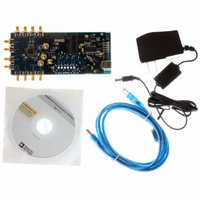
Manufacturer Part Number
AD9516-4/PCBZ
Description
BOARD EVAL FOR AD9516-4 1.8GHZ
Manufacturer
Analog Devices Inc
Specifications of AD9516-4/PCBZ
Main Purpose
Timing, Clock Generator
Embedded
No
Utilized Ic / Part
AD9516-4
Primary Attributes
2 Inputs, 14 Outputs, 1.6GHz VCO
Secondary Attributes
CMOS, LVDS, LVPECL Output Logic, ADIsimCLK™ Graphical User Interface
Silicon Manufacturer
Analog Devices
Application Sub Type
PLL Clock Synthesizer
Kit Application Type
Clock & Timing
Silicon Core Number
AD9516-0, AD9516-1, AD9516-2
Silicon Family Name
AD9516-X
Rohs Compliant
Yes
Lead Free Status / RoHS Status
Lead free / RoHS Compliant


Parameter
CHARGE PUMP (CP)
PRESCALER (PART OF N DIVIDER)
PLL DIVIDER DELAYS
NOISE CHARACTERISTICS
PLL DIGITAL LOCK DETECT WINDOW
1
2
REFIN and REFIN self-bias points are offset slightly to avoid chatter on an open input condition.
For reliable operation of the digital lock detect, the period of the PFD frequency must be greater than the unlock-after-lock time.
I
I
Sink-and-Source Current Matching
I
I
Prescaler Input Frequency
Prescaler Output Frequency
000
001
010
011
100
101
110
111
In-Band Phase Noise of the Charge
PLL Figure of Merit (FOM)
Required to Lock (Coincidence of Edges)
To Unlock After Lock (Hysteresis)
CP
CP
CP
CP
High Value
Low Value
Absolute Accuracy
CP
P = 1 FD
P = 2 FD
P = 3 FD
P = 2 DM (2/3)
P = 4 DM (4/5)
P = 8 DM (8/9)
P = 16 DM (16/17)
P = 32 DM (32/33)
Pump/Phase Frequency Detector
(In-Band Is Within the LBW of the PLL)
At 500 kHz PFD Frequency
At 1 MHz PFD Frequency
At 10 MHz PFD Frequency
At 50 MHz PFD Frequency
Low Range (ABP 1.3 ns, 2.9 ns)
High Range (ABP 1.3 ns, 2.9 ns)
High Range (ABP 6 ns)
Low Range (ABP 1.3 ns, 2.9 ns)
High Range (ABP 1.3 ns, 2.9 ns)
High Range (ABP 6 ns)
Sink/Source
High Impedance Mode Leakage
vs. CP
vs. Temperature
RSET
Range
V
2
2
Min
Typ
4.8
0.60
2.5
2.7/10
1
2
1.5
2
Off
330
440
550
660
770
880
990
−165
−162
−151
−143
3.5
7.5
3.5
7
15
11
−220
Max
300
600
900
200
1000
2400
3000
3000
300
Rev. A | Page 5 of 80
Unit
mA
mA
%
kΩ
nA
%
%
%
MHz
MHz
MHz
MHz
MHz
MHz
MHz
MHz
MHz
ps
ps
ps
ps
ps
ps
ps
ps
dBc/Hz
dBc/Hz
dBc/Hz
dBc/Hz
ns
ns
ns
ns
ns
ns
dBc/Hz
Test Conditions/Comments
Programmable
With CP
CP
0.5 < CP
0.5 < CP
CP
See the
A, B counter input frequency (prescaler input frequency divided
by P)
Register 0x019: R, Bits[5:3], N, Bits[2:0]; see Table 54
The PLL in-band phase noise floor is estimated by measuring the
in-band phase noise at the output of the VCO and subtracting
20log(N) (where N is the value of the N divider)
Reference slew rate > 0.25 V/ns; FOM + 10log (f
mation of the PFD/CP in-band phase noise (in the flat region)
inside the PLL loop bandwidth; when running closed loop, the
phase noise, as observed at the VCO output, is increased by 20log(N)
Signal available at LD, STATUS, and REFMON pins when selected
by appropriate register settings
Selected by Register 0x017[1:0] and Register 0x018[4]
Register 0x017[1:0] = 00b, 01b,11b; Register 0x018[4] = 1b
Register 0x017[1:0] = 00b, 01b, 11b; Register 0x018[4] = 0b
Register 0x017[1:0] = 10b; Register 0x018[4] = 0b
Register 0x017[1:0] = 00b, 01b, 11b; Register 0x018[4] = 1b
Register 0x017[1:0] = 00b, 01b, 11b; Register 0x018[4] = 0b
Register 0x017[1:0] = 10b; Register 0x018[4] = 0b
V
V
= V
= V
CP
CP
RSET
VCXO/VCO Feedback Divider N—P, A, B, R
V
V
/2
/2
< V
< V
= 5.1 kΩ
CP
CP
− 0.5 V
− 0.5 V
PFD
AD9516-4
) is an approxi-
section
Related parts for AD9516-4/PCBZ
Image
Part Number
Description
Manufacturer
Datasheet
Request
R

Part Number:
Description:
IC CLOCK PLL/VCO 2GHZ 64LFCSP
Manufacturer:
Analog Devices Inc
Datasheet:
Part Number:
Description:
IC CLOCK GEN 2.8GHZ VCO 64-LFCSP
Manufacturer:
Analog Devices Inc
Datasheet:
Part Number:
Description:
IC,Fourteen Distributed-Output Clock Driver,LLCC,64PIN,PLASTIC
Manufacturer:
Analog Devices Inc
Datasheet:
Part Number:
Description:
IC,Ten Distributed-Output Clock Driver,LLCC,64PIN,PLASTIC
Manufacturer:
Analog Devices Inc
Datasheet:
Part Number:
Description:
IC,Ten Distributed-Output Clock Driver,LLCC,64PIN,PLASTIC
Manufacturer:
Analog Devices Inc
Datasheet:
Part Number:
Description:
Clock IC With 1.8GHz On-chip VCO
Manufacturer:
Analog Devices Inc
Datasheet:

Part Number:
Description:
BOARD EVAL FOR AD9516-2 2.2GHZ
Manufacturer:
Analog Devices Inc
Datasheet:

Part Number:
Description:
Clock IC With 2.5GHz On-chip VCO EB
Manufacturer:
Analog Devices Inc
Datasheet:
Part Number:
Description:
IC CLOCK GEN 2.8GHZ VCO 64-LFCSP
Manufacturer:
Analog Devices Inc
Datasheet:
Part Number:
Description:
IC,Ten Distributed-Output Clock Driver,LLCC,64PIN,PLASTIC
Manufacturer:
Analog Devices Inc
Datasheet:
Part Number:
Description:
IC,Fourteen Distributed-Output Clock Driver,LLCC,64PIN,PLASTIC
Manufacturer:
Analog Devices Inc
Datasheet:
Part Number:
Description:
IC,Ten Distributed-Output Clock Driver,LLCC,64PIN,PLASTIC
Manufacturer:
Analog Devices Inc
Datasheet:
Part Number:
Description:
Clock IC With 1.8GHz On-chip VCO
Manufacturer:
Analog Devices Inc
Datasheet:
Part Number:
Description:
10/14 Chan Clock IC W/PLL-no VCO
Manufacturer:
Analog Devices Inc
Datasheet:
Part Number:
Description:
10/14 Chan Clock IC W/PLL-no VCO
Manufacturer:
Analog Devices Inc
Datasheet: