LSN2-T/10-D12N-C Murata Power Solutions Inc, LSN2-T/10-D12N-C Datasheet - Page 10
LSN2-T/10-D12N-C
Manufacturer Part Number
LSN2-T/10-D12N-C
Description
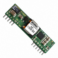
CONV DC/DC 50W 10A 0.75-5V SIP
Manufacturer
Murata Power Solutions Inc
Series
LSN2r
Type
Point of Load (POL) Non-Isolatedr
Datasheet
1.LSN2-T10-W3N-C.pdf
(15 pages)
Specifications of LSN2-T/10-D12N-C
Number Of Outputs
1
Output
0.75 ~ 5V
Power (watts)
50W
Mounting Type
Through Hole
Voltage - Input
8.3 ~ 14V
Package / Case
12-SIP Module
1st Output
0.75 ~ 5 VDC @ 10A
Size / Dimension
2.00" L x 0.32" W x 0.50" H (50.8mm x 8.1mm x 12.7mm)
Power (watts) - Rated
50W
Operating Temperature
-40°C ~ 85°C
Efficiency
95%
Approvals
CSA, EN, UL
Output Power
50 W
Input Voltage Range
8.3 V to 14 V
Input Voltage (nominal)
12 V
Output Voltage (channel 1)
0.75 V to 5 V
Output Current (channel 1)
10 A
Package / Case Size
SIP
Output Type
Low Voltage Selectable
Output Voltage
0.75 V to 5 V
Product
Non-Isolated / POL
Lead Free Status / RoHS Status
Lead free / RoHS Compliant
3rd Output
-
2nd Output
-
Lead Free Status / Rohs Status
Lead free / RoHS Compliant
Other names
811-1801
Available stocks
Company
Part Number
Manufacturer
Quantity
Price

Part Number:
LSN2-T/10-D12N-C
Manufacturer:
MURATA/村田
Quantity:
20 000


Timing is Everything
This mix of system voltages is being distributed by several local power solu-
tions including Point-of-load (POL) DC/DC converters and sometimes a linear
regulator, all sourced from a master AC power supply. While this mix of volt-
ages is challenging enough, a further diffi culty is the start-up and shutdown
timing relationship between these power sources and relative voltage differ-
ences between them.
strap loaded and stabilized before the I/O section is turned on. This avoids
uncommanded data bytes being transferred, compromising an active external
network or placing the I/O section in an undefi ned mode. Or it keeps bad com-
mands out of disk and peripheral controllers until they are ready to go to work.
to the master source all at once. A more serious reason to manage the timing
and voltage differences is to avoid either a latchup condition in program-
mable logic (a latchup might ignore commands or would respond improperly
to them) or a high current startup situation (which may damage on-board
circuits). And on the power down phase, inappropriate timing or voltages can
cause interface logic to send a wrong “epitaph” command.
Two Approaches
There are two ways to manage these timing and voltage differences. Either
the power up/down sequence can be controlled by discrete On/Off logic con-
trols for each power supply (see Figure 7). Or the power up/down cycle is set
by Sequencing or Tracking circuits. Some systems combine both methods.
For many systems, the CPU and memory must be powered up, boot-
Another goal for staggered power-up is to avoid an oversize load applied
STARTUP SEQUENCE:
CPU
POL A
POL B
ENABLE
Figure 7. Power Up/Down Sequencing Controller
SEQUENCING
CONTROLLER
“ALL ON”
OFF
OFF
+12Vdc
TO OTHER POLs
Settling
Delay
ON
ENABLE
ENABLE
+V
+V
IN
IN
ON
POL
POL
A
B
+5V
LOADS
+3.3V
LOADS
TIME
www.murata-ps.com
powered logic sequencer or dedicated microcontroller which turns on each
downstream power section in cascaded series. This of course assumes all
POL’s have On/Off controls. A distinct advantage of the sequencing controller
is that it can produce an “All On” output signal to state that the full system is
stable and ready to go to work. For additional safety, the sequencer can moni-
tor the output voltages of all downstream POL’s with an A/D converter system.
extra cost, wiring and programming complexity. First, power is applied as a
fast-rising, all-or-nothing step which may be unacceptable to certain circuits,
especially large output bypass capacitors. These could force POL’s into
overcurrent shutdown. And some circuits (such as many linear regulators and
some POLs) may not have convenient start-up controls. This requires design-
ing and fabricating external power controls such as high-current MOSFET’s.
must be characterized for start-up and down times. These often vary—one
POL may stabilize in 15 milliseconds whereas another takes 50 milliseconds.
Another problem is that the sequencing controller itself must be “already
running” and stabilized before starting up other circuits. If there is a glitch in
the system, the power up/down sequencer could get out of step with possible
disastrous results. Lastly, changing the timing may require reprogramming the
logic sequencer or rewriting software.
Sequence/Track Input
A different power sequencing solution is employed on MPS’s LSN2 DC/DC
converter. After external input power is applied and the converter stabilizes,
a high impedance Sequence/Track input pin accepts an external analog volt-
age. The output power voltage will then track this Sequence/Track input at a
one-to-one ratio up to the nominal set point voltage for that converter. This
Sequencing input may be ramped, delayed, stepped or otherwise phased as
needed for the output power, all fully controlled by the user’s simple external
circuits. As a direct input to the converter’s feedback loop, response to the
Sequence/Track input is very fast (milliseconds).
On/Off logic sequencer may be duplicated. The Sequence pin system does
not use the converter’s Enable On/Off control (unless it is a master emergency
shut down system).
Power Phasing Architectures
Observe the simplifi ed timing diagrams below. There are many possible power
phasing architectures and these are just some examples to help you analyze
your system. Each application will be different. Multiple output voltages may
require more complex timing than that shown here.
typical power output voltages. Generally the Master will be a primary power
voltage in the system which must be present fi rst or coincident with any
Slave power voltages. The Master output voltage is connected to the Slave’s
Sequence input, either by a voltage divider, divider-plus-capacitor or some
The fi rst system (discrete On/Off controls) applies signals from an already-
However the sequencer controller has some obvious diffi culties besides
If the power up/down timing needs to be closely controlled, each POL
By properly controlling this Sequence pin, most operations of the discrete
These diagrams illustrate the time and slew rate relationship between two
Selectable-Output DC/DC Converters
25 Jun 2010
Non-isolated, DOSA-SIP, 6/10/16A
LSN2 Series
MDC_LSN2.B07Δ
email: sales@murata-ps.com
Page 10 of 15
Related parts for LSN2-T/10-D12N-C
Image
Part Number
Description
Manufacturer
Datasheet
Request
R

Part Number:
Description:
CONV DC/DC 33W 10A .75-3.3V SIP
Manufacturer:
Murata Power Solutions Inc
Datasheet:

Part Number:
Description:
CONV DC/DC 33W 10A .75-3.3V SIP
Manufacturer:
Murata Power Solutions Inc
Datasheet:

Part Number:
Description:
CONV DC/DC 50W 10A 0.75-5V SIP
Manufacturer:
Murata Power Solutions Inc
Datasheet:

Part Number:
Description:
DC/DC Converter
Manufacturer:
Murata Power Solutions Inc
Datasheet:
Part Number:
Description:
DC/DC Converter
Manufacturer:
Murata Power Solutions Inc
Datasheet:
Part Number:
Description:
DC/DC Converter
Manufacturer:
Murata Power Solutions Inc
Datasheet:
Part Number:
Description:
DC/DC Converter
Manufacturer:
Murata Power Solutions Inc
Datasheet:

Part Number:
Description:
DC/DC Converters & Regulators 12Vin 0.8-5Vout 30A 150W Power Good Out
Manufacturer:
Murata Power Solutions Inc
Datasheet:

Part Number:
Description:
DC/DC Converters & Regulators 12Vin 0.8-5Vout 22A 112W NonIso DOSA-SIP
Manufacturer:
Murata Power Solutions Inc
Datasheet:
Part Number:
Description:
DC/DC Converters & Regulators 12Vin 0.8-5Vout 22A 112W Neg polarity
Manufacturer:
Murata Power Solutions Inc
Datasheet:

Part Number:
Description:
Transformers 5Vin 5Vout 200mA 4000Vdc 1:1.33 turn
Manufacturer:
Murata Power Solutions Inc
Datasheet:

Part Number:
Description:
POWER SUPPLY
Manufacturer:
Murata Power Solutions Inc
Datasheet:

Part Number:
Description:
DPM LED MINI 2VDC 3.5DIG LP RED
Manufacturer:
Murata Power Solutions Inc
Datasheet:

Part Number:
Description:
CONV DC/DC 1W 5VIN 5VOUT SIP SGL
Manufacturer:
Murata Power Solutions Inc
Datasheet:

Part Number:
Description:
CONV DC/DC 1W 5VIN 3.3V SIP SGL
Manufacturer:
Murata Power Solutions Inc
Datasheet: