LSM2-T/6-W3N-C Murata Power Solutions Inc, LSM2-T/6-W3N-C Datasheet - Page 14
LSM2-T/6-W3N-C
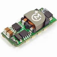
Manufacturer Part Number
LSM2-T/6-W3N-C
Description
CONV DC/DC 19.8W 6A 5V SMD
Manufacturer
Murata Power Solutions Inc
Series
LSM2r
Type
Point of Load (POL) Non-Isolatedr
Datasheet
1.LSM2-T6-W3N-C.pdf
(17 pages)
Specifications of LSM2-T/6-W3N-C
Output
0.75 ~ 3.3V
Number Of Outputs
1
Power (watts)
19W
Mounting Type
Surface Mount
Voltage - Input
2.4 ~ 5.5V
Package / Case
8-DIP SMD Module
1st Output
0.75 ~ 3.3 VDC @ 6A
Size / Dimension
1.30" L x 0.53" W x 0.34" H (33mm x 13.5mm x 8.6mm)
Power (watts) - Rated
19.8W
Operating Temperature
-40°C ~ 85°C
Efficiency
95.5%
Approvals
CSA, cUL, EN, UL
Dc / Dc Converter O/p Type
Variable
No. Of Outputs
1
Input Voltage
2.4V To 5.5V
Power Rating
19.8W
Output Voltage
5V
Output Current
6A
Approval Bodies
UL, CSA
Supply Voltage
5V
Product
Non-Isolated / POL
Output Power
20 W
Input Voltage Range
2.4 V to 5.5 V
Output Voltage (channel 1)
0.75 V to 3.3 V
Output Current (channel 1)
6 A
Lead Free Status / RoHS Status
Lead free / RoHS Compliant
3rd Output
-
2nd Output
-
Lead Free Status / Rohs Status
Lead free / RoHS Compliant
Other names
811-1782-2
Available stocks
Company
Part Number
Manufacturer
Quantity
Price

Part Number:
LSM2-T/6-W3N-C
Manufacturer:
MURATA/村田
Quantity:
20 000


Operation
To use the Sequence pin after power start-up stabilizes, apply a rising external
voltage to the Sequence input. As the voltage rises, the output voltage will
track the Sequence input (gain = 1). The output voltage will stop rising when it
reaches the normal set point for the converter. The Sequence input may option-
ally continue to rise without any effect on the output. Keep the Sequence input
voltage below the converter’s input supply voltage.
until the Sequence input falls below the set point.
below show simple RC networks but you may also use operational amplifi ers,
D/A converters, etc.
Circuits
The circuits shown in Figures 14 through 16 introduce several concepts when
using these Sequencing controls on Point-of-Load (POL) converters. These
circuits are only for reference and are not intended as fi nal designs ready for
your application. Also, numerous connections are omitted for clarity.
POL B ramps up identically to POL A as shown in timing diagram, Figure 10. RC
network R1 and C1 charge up at a rate set by the R1-C1 time constant, giving
a roughly linear ramp. As POL A reaches 3.3V
B will stop rising. POL A then continues rising until it reaches 5V. R1 should be
signifi cantly smaller than the internal bias current resistor from the Sequence
pin. Start with a 20k: value. We assume that the critical phase is only on
power up therefore there is no provision for ramped power down.
Use a similar strategy on power down. The output voltage will stay constant
Any strategy may be used to deliver the power up/down ramps. The circuits
Figure 14 shows a basic Master (POL A) and Slave (POL B) connected so the
Figure 14. Wiring for Simultaneous Phasing
OUT
(the setpoint of POL B), POL
www.murata-ps.com
added a FET at Q1 as an up/down control. When V
POL, Q1 is biased on, shorting out the Sequence pin. When Q1’s gate is biased
off, R1 charges C1 and the POL’s output ramps up at the R1-C1 slew rate. Note:
Q1’s gate would typically be controlled from some external digital logic.
small resistor in series with Q1’s drain.
ing divider (R2 and R3) on POL B. We have also added an optional very small
noise fi lter cap at C2. Figure 16’s circuit corresponds roughly to Figure 11’s
timing for power up.
Figure 15 shows a single POL and the same RC network. However, we have
If you wish to have a ramped power down (rather than a step down), add a
Figure 16 shows both a RC ramp on Master POL A and a proportional track-
Selectable-Output POL DC/DC Converters
Figure 16. Proportional Phasing
Figure 15. Self-Ramping Power Up
25 Jun 2010
Single Output, Non-Isolated
MDC_LSM2
LSM2 Series
email: sales@murata-ps.com
IN
power is applied to the
Series.B09Δ
Page 14 of 17
Related parts for LSM2-T/6-W3N-C
Image
Part Number
Description
Manufacturer
Datasheet
Request
R

Part Number:
Description:
CONV DC/DC 30W 6A 12V SMD
Manufacturer:
Murata Power Solutions Inc
Datasheet:
Part Number:
Description:
CONV DC/DC 19.8W 6A 5V SMD
Manufacturer:
Murata Power Solutions Inc
Datasheet:
Part Number:
Description:
CONV DC/DC 30W 6A 12V SMD
Manufacturer:
Murata Power Solutions Inc
Datasheet:

Part Number:
Description:
DC/DC Converter
Manufacturer:
Murata Power Solutions Inc
Datasheet:
Part Number:
Description:
DC/DC Converter
Manufacturer:
Murata Power Solutions Inc
Datasheet:
Part Number:
Description:
DC/DC Converter
Manufacturer:
Murata Power Solutions Inc
Datasheet:
Part Number:
Description:
DC/DC Converter
Manufacturer:
Murata Power Solutions Inc
Datasheet:

Part Number:
Description:
CONV DC/DC 125W 30A 12V SMD
Manufacturer:
Murata Power Solutions Inc
Datasheet:
Part Number:
Description:
CONV DC/DC 125W 30A 12V SMD
Manufacturer:
Murata Power Solutions Inc
Datasheet:
Part Number:
Description:
CONV DC/DC 33W 10A 5V SMD
Manufacturer:
Murata Power Solutions Inc
Datasheet:

Part Number:
Description:
DC/DC Converter
Manufacturer:
Murata Power Solutions Inc
Datasheet:

Part Number:
Description:
Transformers 5Vin 5Vout 200mA 4000Vdc 1:1.33 turn
Manufacturer:
Murata Power Solutions Inc
Datasheet:

Part Number:
Description:
POWER SUPPLY
Manufacturer:
Murata Power Solutions Inc
Datasheet:

Part Number:
Description:
DPM LED MINI 2VDC 3.5DIG LP RED
Manufacturer:
Murata Power Solutions Inc
Datasheet:

Part Number:
Description:
CONV DC/DC 1W 5VIN 5VOUT SIP SGL
Manufacturer:
Murata Power Solutions Inc
Datasheet: