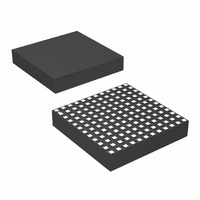
LTM4619EV#PBF Linear Technology, LTM4619EV#PBF Datasheet - Page 4

LTM4619EV#PBF
Manufacturer Part Number
LTM4619EV#PBF
Description
IC SWIT REG BUCK 4A ADJ 144LGA
Manufacturer
Linear Technology
Series
µModuler
Type
Point of Load (POL) Non-Isolatedr
Datasheet
1.LTM4619EVPBF.pdf
(24 pages)
Specifications of LTM4619EV#PBF
Design Resources
LTM4619 Spice Model
Output
0.8 ~ 5 V
Number Of Outputs
2
Power (watts)
30W
Mounting Type
Surface Mount
Voltage - Input
4.5 ~ 26.5 V
Package / Case
144-LGA
1st Output
0.8 ~ 5 VDC @ 4A
2nd Output
0.8 ~ 5 VDC @ 4A
Size / Dimension
0.59" L x 0.59" W x 0.11" H (15mm x 15mm x 2.8mm)
Power (watts) - Rated
30W
Operating Temperature
-40°C ~ 125°C
Lead Free Status / RoHS Status
Lead free / RoHS Compliant
3rd Output
-
Available stocks
Company
Part Number
Manufacturer
Quantity
Price
elecTrical characTerisTics
LTM4619
operating temperature range, otherwise specifications are at T
Specified as each channel. (Note 3)
Note 1: Stresses beyond those listed under Absolute Maximum Ratings
may cause permanent damage to the device. Exposure to any Absolute
Maximum Rating condition for extended periods may affect device
reliability and lifetime.
Note 2: The LTM4619E is guaranteed to meet performance specifications
over the 0°C to 125°C internal operating temperature range. Specifications
over the full –40°C to 125°C internal operating temperature range are
assured by design, characterization and correlation with statistical process
controls. The LTM4619I is guaranteed to meet specifications over the full
Typical perForMance characTerisTics
SYMBOL
f
f
f
R
I
V
R
V
I
ΔV
4
NOM
LOW
HIGH
FREQ
PGOOD
RUN1, 2
PGL
MODE/PLLIN
FB1
PGOOD
, R
95
90
85
80
75
70
65
60
55
FB2
0
Efficiency vs Load Current with
5V
1.2V
IN
0.5
OUT
(f = 500kHz for 0.8V
1
and 1.5V
LOAD CURRENT (A)
2.5V
PARAMETER
Nominal Frequency
Lowest Frequency
Highest Frequency
MODE/PLLIN Input Resistance
Frequency Setting
Sinking Current
Sourcing Current
RUN Pin ON/OFF Threshold
Resistor Between V
Pins for Each Channel
PGOOD Voltage Low
PGOOD Leakage Current
PGOOD Range
1.5
1.2V
OUT
2
0.8V
OUT
OUT
2.5
OUT
)
OUT
3
1.5V
3.3V
,
OUT
3.5
OUT
4619 G01
OUT
and V
4
FB
95
90
85
80
75
70
65
60
55
CONDITIONS
V
V
V
f
f
RUN Rising
RUN Falling
I
V
V
V
MODE
MODE
PGOOD
FREQ
FREQ
FREQ
PGOOD
FB
FB
0
Efficiency vs Load Current with
12V
1.5V
Ramping Negative
Ramping Positive
3.3V
0.5
= 1.2V
= 0V
≥ 2.4V
> f
< f
IN
= 2mA
OUT
OUT
= 5V
The
OSC
OSC
(f = 500kHz for 1.2V
)
1
A
1.5V
LOAD CURRENT (A)
l
5V
= 25°C, V
1.5
denotes the specifications which apply over the full internal
OUT
OUT
internal operating temperature range. Note that the maximum ambient
temperature consistent with these specifications is determined by specific
operating conditions in conjunction with board layout, the rated package
thermal resistance and other environmental factors.
Note 3: The two outputs are tested separately and the same testing
condition is applied to each output.
Note 4: 100% tested at wafer level only.
Note 5: See Output Current Derating curves for different V
2
2.5
IN
1.2V
= 12V (Note 2). Per typical application in Figure 18.
2.5V
3
OUT
OUT
OUT
3.5
(Refer to Figures 18 and 19)
and
4619 G02
4
95
90
85
80
75
70
65
60
55
50
45
0
Efficiency vs Load Current with
24V
0.5
IN
3.3V
(f = 500kHz for 1.5V
1.02
60.1
MIN
450
210
700
1.1
OUT
–5
1
5
LOAD CURRENT (A)
1.5
2.5V
1.22
1.14
60.4
–7.5
OUT
TYP
500
250
780
250
–13
0.1
7.5
13
2
2.5
5V
IN
OUT
MAX
, V
1.35
1.27
60.7
550
290
860
–10
1.5V
0.3
±2
10
OUT
3
OUT
OUT
and T
3.5
)
UNITS
4619 G03
4619fa
kHz
kHz
kHz
kΩ
kΩ
µA
µA
µA
A
4
%
%
.
V
V
V


