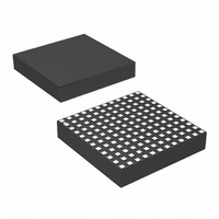
LTM4619EV#PBF Linear Technology, LTM4619EV#PBF Datasheet - Page 13

LTM4619EV#PBF
Manufacturer Part Number
LTM4619EV#PBF
Description
IC SWIT REG BUCK 4A ADJ 144LGA
Manufacturer
Linear Technology
Series
µModuler
Type
Point of Load (POL) Non-Isolatedr
Datasheet
1.LTM4619EVPBF.pdf
(24 pages)
Specifications of LTM4619EV#PBF
Design Resources
LTM4619 Spice Model
Output
0.8 ~ 5 V
Number Of Outputs
2
Power (watts)
30W
Mounting Type
Surface Mount
Voltage - Input
4.5 ~ 26.5 V
Package / Case
144-LGA
1st Output
0.8 ~ 5 VDC @ 4A
2nd Output
0.8 ~ 5 VDC @ 4A
Size / Dimension
0.59" L x 0.59" W x 0.11" H (15mm x 15mm x 2.8mm)
Power (watts) - Rated
30W
Operating Temperature
-40°C ~ 125°C
Lead Free Status / RoHS Status
Lead free / RoHS Compliant
3rd Output
-
Available stocks
Company
Part Number
Manufacturer
Quantity
Price
applicaTions inForMaTion
Multiphase Operation
Multiphase operation with multiple LTM4619 devices in
parallel will lower the effective input RMS ripple current
as well as the output ripple current due to the interleaving
operation of the regulators. Figure 5 provides a ratio of
input RMS ripple current to DC load current as a function
of duty cycle and the number of paralleled phases. Choose
the corresponding duty factor and the number of phases
to get the correct ripple current value. For example, the
2-phase parallel for one LTM4619 design provides 8A
at 2.5V output from a 12V input. The duty cycle is DC =
2.5V/12V = 0.21. The 2-phase curve has a ratio of ~0.25
for a duty cycle of 0.21. This 0.25 ratio of RMS ripple cur-
rent to a DC load current of 8A equals ~2A of input RMS
ripple current for the external input capacitors.
The effective output ripple current is lowered with mul-
tiphase operations as well. Figure 6 provides a ratio of
peak-to-peak output ripple current to the normalized
output ripple current as a function of duty factor and the
number of paralleled phases. Choose the corresponding
duty factor and the number of phases to get the correct
output ripple current ratio value. If a 2-phase operation
is chosen at 12V
then 0.6 is the ratio of the normalized output ripple current
to inductor ripple DIr at the zero duty factor. This leads
to ~1.3A of the effective output ripple current ΔI
DIr is at 2.2A. Refer to Application Note 77 for a detailed
explanation of the output ripple current reduction as a
function of paralleled phases.
The output voltage ripple has two components that are
related to the amount of bulk capacitance and effective
series resistance (ESR) of the output bulk capacitance.
Therefore, the output voltage ripple can be calculated with
the known effective output ripple current. The equation:
where f is frequency and N is the number of parallel phases.
ΔV
OUT(P-P)
≈ ΔI
IN
L
to 2.5V
/(8 • f • N • C
OUT
with a duty factor of 21%,
OUT
) + ESR • ΔI
L
L
if the
RUN Pin
The RUN pins can be used to enable or sequence the
particular regulator channel. The RUN pins have their
own internal 0.5µA current source to pull up the pin to
1.2V, and then the current increases to 4.5µA above 1.2V.
Careful consideration is needed to assure that board
contamination or residue does not load down the 0.5µA
pull-up current. Otherwise active control to these pins can
be used to activate the regulators. A voltage divider can
be used from V
as a UVLO feature for the regulator. The resistor divider
needs to be low enough resistance to swamp out the pull-
up current sources and not enable the device when not
attended. See the Simplified Block Diagram.
Power Good
The PGOOD pin is connected to an open drain of an internal
N-channel MOSFET. The MOSFET turns on and pulls the
PGOOD pin low when either V
±7.5% of the 0.8V reference voltage. The PGOOD pin is
also pulled low when either RUN pin is below 1.2V or when
the LTM4619 is in the soft-start or tracking phase. When
the V
MOSFET is turned off and the pin is allowed to be pulled
up by an external resistor to a source of up to 6V. The
PGOOD pin will flag power good immediately when both
V
an internal 17µs power bad mask when either V
out of the ±7.5% window.
FB
pins are within the ±7.5% window. However, there is
FB
pin voltage is within the ±7.5% requirement, the
IN
to set an enable point that can be used
FB
pin voltage is not within
LTM4619
FB
13
goes
4619fa


