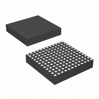
LTM4619EV#PBF Linear Technology, LTM4619EV#PBF Datasheet

LTM4619EV#PBF
Specifications of LTM4619EV#PBF
Available stocks
Related parts for LTM4619EV#PBF
LTM4619EV#PBF Summary of contents
Page 1
... Industrial Equipment n Point of Load Regulation n L, LT, LTC, LTM, Linear Technology, the Linear logo, Burst Mode and µModule are registered trademarks and LTpowerCAD is a trademark of Linear Technology Corporation. All other trademarks are the property of their respective owners. Typical applicaTion Dual 4A 3.3V/2.5V DC/DC µModule ...
Page 2
... Storage Temperature Range .................. –55°C to 125°C orDer inForMaTion LEAD FREE FINISH TRAY LTM4619EV#PBF LTM4619EV#PBF LTM4619IV#PBF LTM4619IV#PBF Consult LTC Marketing for parts specified with wider operating temperature ranges. *The temperature grade is identified by a label on the shipping container. For more information on lead free part marking, go to: This product is only offered in trays ...
Page 3
T Specified as each channel. (Note 3) SYMBOL PARAMETER I Input Inrush Current at Start-Up INRUSH(VIN) I Input Supply Bias Current Q(VIN) I Input Supply Current S(VIN) INTV Internal V Voltage ...
Page 4
LTM4619 elecTrical characTerisTics operating temperature range, otherwise specifications are at T Specified as each channel. (Note 3) SYMBOL PARAMETER f Nominal Frequency NOM f Lowest Frequency LOW f Highest Frequency HIGH R MODE/PLLIN Input Resistance MODE/PLLIN I Frequency Setting FREQ ...
Page 5
Typical perForMance characTerisTics 1.2V Output Transient Response I OUT 1A/DIV V OUT 50mV/DIV 100µs/DIV 4619 G04 6V 1.2V AT 2A/µs LOAD STEP IN OUT f = 780kHz C 2× 22µF, 6.3V X5R CERAMIC OUT C 1× 330µF, 6.3V SANYO POSCAP ...
Page 6
LTM4619 pin FuncTions V (J1 to J3, J10 to J12 K4 K12 L5 L12 M12): Power Input Pins. Apply input voltage between these pins and PGND pins. Recommend placing ...
Page 7
DiagraM INTV CC PGOOD MODE/PLLIN EXTV TK/SS1 C SS1 R1 RUN1 COMP1 R2 R2 • V IN R1+ R2 TK/SS2 = UVLO THRESHOLD = 1.22V C SS2 RUN2 COMP2 ...
Page 8
LTM4619 operaTion The LTM4619 is a dual-output standalone non-isolated switching mode DC/DC power supply. It can deliver (DC current) for each output with few external input and output capacitors. This module provides precisely regulated output voltages programmable ...
Page 9
The typical LTM4619 application circuit is shown in Figure 18. External component selection is primarily deter- mined by the maximum load current and output voltage. Output Voltage Programming The PWM controller has an internal 0.8V reference voltage. As ...
Page 10
LTM4619 applicaTions inForMaTion Mode Selections and Phase-Locked Loop The LTM4619 can be enabled to enter high efficiency Burst Mode operation, constant-frequency pulse-skipping mode, or forced continuous conduction mode. To select the forced continuous operation, tie the MODE/PLLIN pin to a ...
Page 11
Soft-Start and Tracking The LTM4619 has the ability to either soft-start by itself with a capacitor or track the output of another channel or external supply. When one particular channel is configured to soft-start by itself, a capacitor ...
Page 12
LTM4619 applicaTions inForMaTion 0.60 0.55 0.50 0.45 0.40 0.35 0.30 0.25 0.20 0.15 0.10 0.05 0 0.1 0.15 0.2 0.25 0.3 0.35 0.4 0.45 0.5 0.55 0.6 0.65 0.7 0.75 0.8 0.85 0.9 Figure 5. Normalized Input RMS Ripple Current ...
Page 13
Multiphase Operation Multiphase operation with multiple LTM4619 devices in parallel will lower the effective input RMS ripple current as well as the output ripple current due to the interleaving operation of the regulators. Figure 5 provides a ratio ...
Page 14
LTM4619 applicaTions inForMaTion INTV and EXTV CC CC The INTV is the internal 5V regulator that powers the CC LTM4619 internal circuitry and drives the power MOSFETs. The input voltage of the LTM4619 must above for the ...
Page 15
Table 2. 1.5V Output DERATING CURVE V (V) IN Figures Figures Figures Figures 10 Figures 10 Figures 10 ...
Page 16
LTM4619 applicaTions inForMaTion AMBIENT TEMPERATURE (°C) Figure 9. 6V without Heat Sink ...
Page 17
Layout Checklist/Example The high integration of LTM4619 makes the PCB board layout very simple and easy. However, to optimize its electri- cal and thermal performance, some layout considerations are still necessary. • Use large PCB copper areas for ...
Page 18
LTM4619 Typical applicaTions V IN 4.5V TO 26. 10µF ×2 V OUT1 5V/4A C OUT1 100µF INTV Figure 18. Typical 4.5V to 26.5V Input, 5V and 3.3V Outputs at 4A Design 18 MODE/PLLIN INTV CC V FREQ/PLLFLTR IN ...
Page 19
Typical applicaTions 26.5V 10µF ×2 V OUT1 1.2V/4A C OUT1 100µF ×2 INTV Figure 19. Typical 4.5V to 26.5V Input, 1.2V and 1.5V Outputs at 4A Design with Adjusted Frequency at 500kHz MODE/PLLIN INTV ...
Page 20
LTM4619 Typical applicaTions 26.5V Figure 20. Output Paralleled LTM4619 Module for 5V Output at 8A Design 20 MODE/PLLIN EXTV INTV FREQ/PLLFLTR COMP1 V 10µF FB1 COMP2 V FB2 TK/SS1 V ...
Page 21
Typical applicaTions 26. IN2 IN1 10µF 330µ OUT1 + 5V/4A C2 220µF 2 PHASE OSCILLATOR + V OUT1 C3 GND OUT2 LTC6908-2 R9 0.1µF SET MOD 143k V OUT3 + 2.5V/4A ...
Page 22
LTM4619 package DescripTion PIN NAME A1 V OUT2 A2 V OUT2 A3 V OUT2 A4 GND A5 GND A6 GND A7 GND A8 GND A9 GND A10 V OUT1 A11 V OUT1 A12 V OUT1 B1 V OUT2 B2 V ...
Page 23
... DescripTion Information furnished by Linear Technology Corporation is believed to be accurate and reliable. However, no responsibility is assumed for its use. Linear Technology Corporation makes no representa- tion that the interconnection of its circuits as described herein will not infringe on existing patent rights. LGA Package 144-Lead (15mm × 15mm × 2.82mm) ...
Page 24
... Temperature Sensing Diode Output, 15mm × 15mm × 4.3mm LGA www.linear.com ● ≤ 5V, 15mm × 15mm × 2.8mm LGA OUT ≤ 5V, 15mm × 15mm × 2.8mm LGA OUT ≤ 5.5V, Remote Sense Amplifier, Internal OUT 4619fa LT 0111 REV A • PRINTED IN USA LINEAR TECHNOLOGY CORPORA TION 2009 ...


