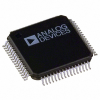
AD5520JST Analog Devices Inc, AD5520JST Datasheet

AD5520JST
Specifications of AD5520JST
Available stocks
Related parts for AD5520JST
AD5520JST Summary of contents
Page 1
FEATURES Force/measure functions FIMV, FVMI, FVMV, FIMI, FNMV Force/measure voltage range ± user programmable force/measure current ranges ±4 μA, ±40 μA, ±400 μA, ±4 mA (external resistors) 2 user programmable extended current ranges without ...
Page 2
AD5520 TABLE OF CONTENTS Features .............................................................................................. 1 Applications....................................................................................... 1 General Description ......................................................................... 1 Functional Block Diagram .............................................................. 1 Specifications..................................................................................... 3 Timing Characteristics..................................................................... 6 Absolute Maximum Ratings............................................................ 7 ESD Caution.................................................................................. 7 Pin Configuration and Function Descriptions............................. 8 Typical Performance Characteristics ........................................... ...
Page 3
SPECIFICATIONS AV = +15 V ± 5 −15 V ± 5 unless otherwise noted. Table 1. Parameter VOLTAGE FORCE MODE Force Control Output Voltage Range FOH Output Impedance FOH0 FOH1 FOH2 FOH3 Input Offset Error ...
Page 4
AD5520 Parameter 4, 5 AMPLIFIER SETTLING TIME V Amp SENSE I Amp SENSE 4, 5 LOOP SETTLING COMPIN2 = 100 pF COMPIN1 = 1000 pF COMPIN0 = 3000 pF SLEW RATE 4, 5 COMPARATOR CPH, CPL Input Range Input Offset ...
Page 5
Parameter POWER REQUIREMENTS Power Supply Rejection Ratio, PSRR 1 FOH MEASOUT DC PSR AVCC I AVEE I DVDD 1 Typical values are at 25°C and nominal supply, unless otherwise noted. 2 Full-scale = ...
Page 6
AD5520 TIMING CHARACTERISTICS AV = +15 V ± 5 −15 V ± 5%, AGND = 0 V, REFGND = 0 V, DGND = 0 V. All specifications 0°C to 70°C, unless otherwise noted. Table ...
Page 7
ABSOLUTE MAXIMUM RATINGS T = 25°C, unless otherwise noted. A Table 3. Parameter Rating AGND −0 AGND +0.3 V, − −0.3 V ...
Page 8
AD5520 PIN CONFIGURATION AND FUNCTION DESCRIPTIONS CPOH CPOL CPCK DGND CLHDETECT CLLDETECT CONNECT Table 4. Pin Function Descriptions Pin No. Mnemonic Description 1 CPH Upper Comparator Threshold Voltage Input, CPH > CPL. 2 CPL Lower Comparator Threshold ...
Page 9
Pin No. Mnemonic Description 23 FSEL Logic Input. Force mode select. Used to select between current or voltage force operation. See the Force Voltage or Force Current section. 24 MSEL Logic Input. Measure mode select. Used to connect MEASOUT to ...
Page 10
AD5520 TYPICAL PERFORMANCE CHARACTERISTICS 0.0030 0.0025 0.0020 0.0015 0.0010 0.0005 TEMPERATURE (°C) Figure 5. Voltage Sense Amplifier Linearity vs. Temperature 100 1k FREQUENCY ...
Page 11
V = +15V –15V SS – 25° –10 COMP –15 – 1.0nF COMP –25 – 3.3nF –35 COMP –40 –45 100 1k 10k FREQUENCY (Hz) Figure 11. Force ...
Page 12
AD5520 +15V –15V 25° –10 –20 –30 –40 –50 –60 100k 1M FREQUENCY (Hz) Figure 17. Voltage Sense Amplifier AC PSRR 700 600 GUARD 500 400 V 300 ...
Page 13
THEORY OF OPERATION The AD5520 is a single-channel per pin parametric measure- ment unit (PPMU) for use in semiconductor automatic test equipment. It contains programmable modes to force a pin voltage and measure the corresponding current (FVMI), force current measure ...
Page 14
AD5520 INTERFACE The AD5520 PPMU is controlled via a number of digital inputs, which are discussed in detail in the following sections. All inputs are TTL-compatible used to select the device while STB (active low input) latches data ...
Page 15
FORCE CONTROL AMPLIFIER The force control amplifier requires external capacitors connected between the COMPOUTx and COMPINx pins. For stability with large capacitance at the DUT, the largest capacitance value (3000 pF) should be selected. The force control amplifier should always ...
Page 16
AD5520 CIRCUIT OPERATION FORCE VOLTAGE Most PMU measurements are performed while in force voltage and measure current modes; for example, when the device is used as a device power supply continuity or leakage testing. In the force voltage ...
Page 17
FORCE CURRENT In force current mode, the voltage at FIN is now converted to a current through the following relationship: Force Current = V /(R × 16) FIN SENSE Figure 24 shows a simplified diagram of the PMU when in ...
Page 18
AD5520 SETTLING TIME CONSIDERATIONS Fast throughput is a key requirement in automatic test equipment because it relates directly to the cost of manufac- turing the DUT; thus reducing the time required to make a measurement is of greatest importance. When ...
Page 19
PCB LAYOUT AND POWER SUPPLY DECOUPLING In any circuit where accuracy is important, careful considera- tion to the power supply and the ground return layout helps to ensure the rated performance. The printed circuit board on which the AD5520 is ...
Page 20
AD5520 TYPICAL CONNECTION CIRCUIT FOR THE AD5520 Figure 26 shows the AD5520 as connected in a typical applica- tion. The external components required are three compensation capacitors and six sense resistors, depending on the number of ranges required. If high ...
Page 21
TYPICAL APPLICATION CIRCUIT Figure 27 shows the AD5520 ATE system. This device can used as a per pin parametric unit in order to speed up the rate at which testing can be done. It can also be ...
Page 22
AD5520 EVALUATION BOARD FOR THE AD5520 A full-featured evaluation kit is available for the AD5520. It includes an evaluation board with direct hookup via a 36-way Centronics connector to a PC. PC-based software to control the AD5520 is also part ...
Page 23
RL2 RELAY–G6H RL1 RELAY–G6H D[0: 12.4Ω R5, 124Ω R4, 1.24kΩ R3, 12.4kΩ R2, 124kΩ R1, Figure 28. Evaluation Board Schematic Rev Page AD5520 ...
Page 24
... ROTATED 90° CCW ORDERING GUIDE Model Temperature Range AD5520JST 0°C to 70°C AD5520JST-REEL 0°C to 70°C 1 AD5520JSTZ-REEL 0°C to 70°C EVAL-AD5520EB Pb-free part. © 2005 Analog Devices, Inc. All rights reserved. Trademarks and registered trademarks are the property of their respective owners. 0.75 0.60 1 ...


