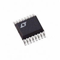
LTC3832EGN Linear Technology, LTC3832EGN Datasheet - Page 18

LTC3832EGN
Manufacturer Part Number
LTC3832EGN
Description
IC DC/DC CTRLR SYNC STPDN 16SSOP
Manufacturer
Linear Technology
Type
Step-Down (Buck)r
Datasheet
1.LTC3832-1ES8PBF.pdf
(24 pages)
Specifications of LTC3832EGN
Internal Switch(s)
No
Synchronous Rectifier
Yes
Number Of Outputs
1
Voltage - Output
2.5V
Current - Output
20A
Frequency - Switching
300kHz
Voltage - Input
3 ~ 8 V
Operating Temperature
-40°C ~ 85°C
Mounting Type
Surface Mount
Package / Case
16-SSOP
Lead Free Status / RoHS Status
Contains lead / RoHS non-compliant
Power - Output
-
Available stocks
Company
Part Number
Manufacturer
Quantity
Price
Company:
Part Number:
LTC3832EGN
Manufacturer:
LT
Quantity:
10 000
Company:
Part Number:
LTC3832EGN#PBF
Manufacturer:
Linear Technology
Quantity:
135
Part Number:
LTC3832EGN#TRPBF
Manufacturer:
LT/凌特
Quantity:
20 000
LTC3832/LTC3832-1
APPLICATIO S I FOR ATIO
1. In general, layout should begin with the location of the
power devices. Be sure to orient the power circuitry so that
a clean power flow path is achieved. Conductor widths
should be maximized and lengths minimized. After you are
satisfied with the power path, the control circuitry should
be laid out. It is much easier to find routes for the relatively
small traces in the control circuits than it is to find
circuitous routes for high current paths.
2. The GND and PGND pins should be shorted directly at
the LTC3832. This helps to minimize internal ground dis-
turbances in the LTC3832 and prevent differences in ground
potential from disrupting internal circuit operation. This
connection should then tie into the ground plane at a single
point, preferably at a fairly quiet point in the circuit such as
close to the output capacitors. This is not always practical,
however, due to physical constraints. Another reasonably
good point to make this connection is between the output
capacitors and the source connection of the bottom
MOSFET Q2. Do not tie this single point ground in the trace
run between the Q2 source and the input capacitor ground,
as this area of the ground plane will be very noisy.
18
4.7 F
C1
C
C
R
U
C
+
U
GND
C
1 F
NC
SS
GND
Figure 11. Typical Schematic Showing Layout Considerations
W
FREQSET
SHDN
COMP
SS
GND
V
CC
LTC3832
100
SENSE
SENSE
PV
PGND
PV
I
CC2
MAX
CC1
G1
I
G2
FB
FB
U
+
–
PV
CC
PGND
NC
1 F
3. The small-signal resistors and capacitors for frequency
compensation and soft-start should be located very close
to their respective pins and the ground ends connected to
the signal ground pin through a separate trace. Do not
connect these parts to the ground plane!
4. The V
be as close to the LTC3832 as possible. The 4.7 F and 1 F
bypass capacitors shown at V
provide optimum regulation performance.
5. The (+) plate of C
possible to the drain of the upper MOSFET, Q1. An additional
1 F ceramic capacitor between V
recommended.
6. The SENSE and V
the switching node. Care should be taken to isolate SENSE
and V
switching signal. Connecting the SENSE
to the load can significantly improve load regulation.
7. Kelvin sense I
0.1 F
FB
CC
from possible capacitive coupling to the inductor
1k
, PV
CC1
MAX
Q1A
and PV
PGND
FB
V
IN
and I
Q2
IN
pins are very sensitive to pickup from
should be connected as close as
CC2
Q1B
FB
+
at Q1’s drain and source pins.
decoupling capacitors should
CC
C
, PV
IN
L
O
IN
CC1
and power ground is
+
+
and PV
3832 F11
and SENSE
C
V
OUT
OUT
CC2
sn3832 3832fs
will help
–
close


