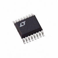
LTC3832EGN Linear Technology, LTC3832EGN Datasheet

LTC3832EGN
Specifications of LTC3832EGN
Available stocks
Related parts for LTC3832EGN
LTC3832EGN Summary of contents
Page 1
... In shutdown mode, the LTC3832 supply current drops to <10 A. The LTC3832-1 is the SO-8 version without current limit, frequency adjustment and shutdown functions. , LTC and LT are registered trademarks of Linear Technology Corporation ...
Page 2
... U (Note 1) Junction Temperature ........................................... 125 C Operating Temperature Range (Note 9) .. – Storage Temperature Range ................. – 150 C Lead Temperature (Soldering, 10 sec).................. 300 ORDER PART NUMBER LTC3832EGN G1 PV CC1 GND GN FB PART MARKING 3832 T JMAX The denotes specifications that apply over the full operating temperature = 25 C ...
Page 3
ELECTRICAL CHARACTERISTICS range, otherwise specifications are at T SYMBOL PARAMETER I Supply Current VCC I PV Supply Current PVCC CC f Internal Oscillator Frequency OSC Minimum Duty Cycle SAWL COMP Maximum Duty Cycle SAWH ...
Page 4
LTC3832/LTC3832 TYPICAL PERFOR A CE CHARACTERISTICS Load Regulation 2. REFER TO FIGURE 12 2.53 2.52 2.51 2.50 2.49 2.48 2.47 2.46 –10 –5 5 – OUTPUT CURRENT (A) 3832 G01 ...
Page 5
W U TYPICAL PERFOR A CE CHARACTERISTICS Maximum G1 Duty Cycle vs Temperature 100 REFER TO FIGURE –50 – 100 125 TEMPERATURE ...
Page 6
LTC3832/LTC3832 TYPICAL PERFOR A CE CHARACTERISTICS PV Supply Current CC vs Gate Capacitance 12V CC1 CC1 ...
Page 7
CTIO S FREQSET (Pin 11/NA): Frequency Set. Use this pin to adjust the free-running frequency of the internal oscillator. With the pin floating, the oscillator runs at about 300kHz. A resistor from FREQSET to ground ...
Page 8
LTC3832/LTC3832-1 W BLOCK DIAGRA (LTC3832-1) INTERNAL OSCILLATOR COMP QSS + V 2.2V QC 1.2V TEST CIRCUITS SHDN CC SHDN CC2 CC1 FREQSET LTC3832 NC ...
Page 9
U U APPLICATIO S I FOR ATIO Also included in the LTC3832 is an internal soft-start feature that requires only a single external capacitor to operate. In addition, the LTC3832 features an adjustable oscillator that can free run or synchronize ...
Page 10
LTC3832/LTC3832 APPLICATIO S I FOR ATIO remains at a reduced voltage until the overload is re- moved. Serious overloads generate a large overdrive at CC, allowing it to pull SS down quickly and preventing damage to the output ...
Page 11
U U APPLICATIO S I FOR ATIO Connecting a 82k resistor from FREQSET to ground forces 15 A out of the pin, causing the internal oscillator to run at approximately 450kHz. Forcing an external 20 A current into FREQSET cuts ...
Page 12
LTC3832/LTC3832 APPLICATIO S I FOR ATIO CC2 CC1 G1 INTERNAL CIRCUITRY G2 LTC3832 Figure 6. LTC3832 Power Supplies V / CC2 CC1 G1 INTERNAL CIRCUITRY G2 LTC3832-1 Figure 7. LTC3832-1 Power Supplies ...
Page 13
U U APPLICATIO S I FOR ATIO Diagram). This increases the G2 on-time and allows the charge pump capacitors to be refreshed. For applications using an external supply to PV supply must also be higher than V ensure normal operation. ...
Page 14
LTC3832/LTC3832 APPLICATIO S I FOR ATIO Note that the required R for Q2 is roughly three DS(ON) times that this example. Note also that while the required R values suggest large MOSFETs, the DS(ON) power ...
Page 15
U U APPLICATIO S I FOR ATIO requirements. Peak current in the inductor will be equal to the maximum output load current plus half of the peak-to- peak inductor ripple current. Ripple current is set by the inductor value, the ...
Page 16
LTC3832/LTC3832 APPLICATIO S I FOR ATIO LTC3832 application might exhibit 5A input ripple cur- rent. Sanyo OS-CON capacitors, part number 10SA220M (220 F/10V), feature 2.3A allowable ripple current three in parallel at the input (to ...
Page 17
U U APPLICATIO S I FOR ATIO between the top of the resistor divider network and the V pin to create a pole-zero pair in the loop compensation. The zero location is prior to the pole location and thus, phase ...
Page 18
LTC3832/LTC3832 APPLICATIO S I FOR ATIO 1. In general, layout should begin with the location of the power devices. Be sure to orient the power circuitry so that a clean power flow path is achieved. Conductor widths should ...
Page 19
U U APPLICATIO S I FOR ATIO OPTIONAL D Z 12V 1N5242 + 10 F 100 + 1 F 4 SHDN 180pF 18k C C 1500pF W U 1N5817 1N5817 0.1 F 5.6k ...
Page 20
LTC3832/LTC3832-1 U TYPICAL APPLICATIO 3. 330 2 SHUTDOWN 68pF 6. 0. Typical 3.3V to 5V, 5A ...
Page 21
U TYPICAL APPLICATIO S Typical 3.3V to – 5V, 5A Positive-to-Negative Converter 100 0.01 F 8.2V NC SHUTDOWN 15k C1 180pF C C 1.5nF V IN 3.3V MBR0520 3.5k ...
Page 22
LTC3832/LTC3832-1 PACKAGE DESCRIPTIO .254 MIN .0165 .0015 RECOMMENDED SOLDER PAD LAYOUT .007 – .0098 (0.178 – 0.249) .016 – .050 (0.406 – 1.270) NOTE: 1. CONTROLLING DIMENSION: INCHES INCHES 2. DIMENSIONS ARE IN (MILLIMETERS) 3. DRAWING NOT TO SCALE *DIMENSION ...
Page 23
... MOLD FLASH OR PROTRUSIONS SHALL NOT EXCEED .006" (0.15mm) Information furnished by Linear Technology Corporation is believed to be accurate and reliable. However, no responsibility is assumed for its use. Linear Technology Corporation makes no represen- tation that the interconnection of its circuits as described herein will not infringe on existing patent rights. ...
Page 24
... Low Input Voltage, High Power Synchronous Controller LTC3831 High Power Synchronous Switching Regulator Controller for DDR Memory Termination trademark of Linear Technology Corporation. SENSE Linear Technology Corporation 24 1630 McCarthy Blvd., Milpitas, CA 95035-7417 (408) 432-1900 FAX: (408) 434-0507 Typical 5V to 3.3V, 10A Application ...


