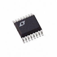
LTC3703EGN-5 Linear Technology, LTC3703EGN-5 Datasheet - Page 7

LTC3703EGN-5
Manufacturer Part Number
LTC3703EGN-5
Description
IC BUCK/BOOST SYNC ADJ 5A 16SSOP
Manufacturer
Linear Technology
Type
Step-Down (Buck), Step-Up (Boost)r
Datasheet
1.LTC3703EGN-5PBF.pdf
(32 pages)
Specifications of LTC3703EGN-5
Internal Switch(s)
No
Synchronous Rectifier
Yes
Number Of Outputs
1
Voltage - Output
0.8 ~ 55.8 V
Current - Output
5A
Frequency - Switching
100kHz ~ 600kHz
Voltage - Input
9.3 ~ 60 V
Operating Temperature
-40°C ~ 85°C
Mounting Type
Surface Mount
Package / Case
16-SSOP
Lead Free Status / RoHS Status
Contains lead / RoHS non-compliant
Power - Output
-
Available stocks
Company
Part Number
Manufacturer
Quantity
Price
Company:
Part Number:
LTC3703EGN-5
Manufacturer:
LT
Quantity:
10 000
Part Number:
LTC3703EGN-5
Manufacturer:
LINEAR/凌特
Quantity:
20 000
Company:
Part Number:
LTC3703EGN-5#PBF
Manufacturer:
LT
Quantity:
320
Part Number:
LTC3703EGN-5#PBF
Manufacturer:
LINEAR/凌特
Quantity:
20 000
Company:
Part Number:
LTC3703EGN-5#TRPBF
Manufacturer:
LT
Quantity:
2 956
Part Number:
LTC3703EGN-5#TRPBF
Manufacturer:
LINEAR/凌特
Quantity:
20 000
PI FU CTIO S
MODE/SYNC (Pin 1/Pin 6): Pulse Skip Mode Enable/Sync
Pin. This multifunction pin provides Pulse Skip Mode en-
able/disable control and an external clock input for synchro-
nization of the internal oscillator. Pulling this pin below 0.8V
or to an external logic-level synchronization signal disables
Pulse Skip Mode operation and forces continuous opera-
tion. Pulling the pin above 0.8V enables Pulse Skip Mode
operation. This pin can also be connected to a feedback
resistor divider from a secondary winding on the inductor
to regulate a second output voltage.
f
this pin sets the free running frequency of the internal os-
cillator. See applications section for resistor value selec-
tion details.
COMP (Pin 3/Pin 8): Loop Compensation. This pin is con-
nected directly to the output of the internal error amplifier.
An RC network is used at the COMP pin to compensate the
feedback loop for optimal transient response.
FB (Pin 4/Pin 9): Feedback Input. Connect FB through a
resistor divider network to V
Also connect the loop compensation network from COMP
to FB.
I
the current limit comparator threshold. If the voltage drop
across the bottom MOSFET exceeds the magnitude of the
voltage at I
I
current threshold to be set with a single external resistor
to ground. See the Current Limit Programming section for
more information on choosing R
INV (Pin 6/Pin 11): Top/Bottom Gate Invert. Pulling this pin
above 2V sets the controller to operate in step-up (boost)
mode with the TG output driving the synchronous MOSFET
and the BG output driving the main switch. Below 1V, the
controller will operate in step-down (buck) mode.
RUN/SS (Pin 7/Pin 13): Run/Soft-Start. Pulling RUN/SS be-
low 0.9V will shut down the LTC3703-5, turn off both of the
external MOSFET switches and reduce the quiescent sup-
ply current to 25µA. A capacitor from RUN/SS to ground
will control the turn-on time and rate of rise of the output
voltage at power-up. An internal 4µA current source pull-
up at the RUN/SS pin sets the turn-on time at approximately
750ms/µF.
SET
MAX
MAX
U
(Pin 2/Pin 7): Frequency Set. A resistor connected to
pin has an internal 12µA current source, allowing the
(Pin 5/Pin 10): Current Limit Set. The I
U
MAX
, the controller goes into current limit. The
U
(GN16/G28)
OUT
to set the output voltage.
IMAX
.
MAX
pin sets
GND (Pin 8/Pin 14): Ground Pin.
BGRTN (Pin 9/Pin 15): Bottom Gate Return. This pin con-
nects to the source of the pull-down MOSFET in the BG
driver and is normally connected to ground. Connecting a
negative supply to this pin allows the synchronous
MOSFET’s gate to be pulled below ground to help prevent
false turn-on during high dV/dt transitions on the SW node.
See the Applications Information section for more details.
BG (Pin 10/Pin 19): Bottom Gate Drive. The BG pin drives
the gate of the bottom N-channel synchronous switch
MOSFET. This pin swings from BGRTN to DRV
DRV
provides power to the BG output driver. This pin should be
connected to a voltage high enough to fully turn on the
external MOSFETs, normally 4.5V to 15V for logic level
threshold MOSFETs. DRV
with a 10µF, low ESR (X5R or better) ceramic capacitor.
V
except the output drivers are powered from this pin. V
should be connected to a low noise power supply voltage
between 4.5V and 15V and should be bypassed to GND
(Pin 8) with at least a 0.1µF capacitor in close proximity to
the LTC3703-5.
SW (Pin 13/Pin 26): Switch Node Connection to Inductor
and Bootstrap Capacitor. Voltage swing at this pin is from
a Schottky diode (external) voltage drop below ground to
V
TG (Pin 14/Pin 27): Top Gate Drive. The TG pin drives the
gate of the top N-channel synchronous switch MOSFET. The
TG driver draws power from the BOOST pin and returns to
the SW pin, providing true floating drive to the top MOSFET.
BOOST (Pin 15/Pin 28): Top Gate Driver Supply. The BOOST
pin supplies power to the floating TG driver. The BOOST pin
should be bypassed to SW with a low ESR (X5R or better)
0.1µF ceramic capacitor. An additional fast recovery Schot-
tky diode from DRV
ing charge-pumped supply at BOOST.
V
nected to the high voltage input of the regulator and is used
by the internal feedforward compensation circuitry to im-
prove line regulation. This is not a supply pin.
CC
IN
IN
.
(Pin 16/Pin 1): Input Voltage Sense Pin. This pin is con-
(Pin 12/Pin 21) : Main Supply Pin. All internal circuits
CC
(Pin 11/Pin 20): Driver Power Supply Pin. DRV
CC
to BOOST will create a complete float-
CC
should be bypassed to BGRTN
LTC3703-5
CC
.
37035fa
7
CC
CC


