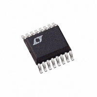
LTC3703EGN-5 Linear Technology, LTC3703EGN-5 Datasheet - Page 23

LTC3703EGN-5
Manufacturer Part Number
LTC3703EGN-5
Description
IC BUCK/BOOST SYNC ADJ 5A 16SSOP
Manufacturer
Linear Technology
Type
Step-Down (Buck), Step-Up (Boost)r
Datasheet
1.LTC3703EGN-5PBF.pdf
(32 pages)
Specifications of LTC3703EGN-5
Internal Switch(s)
No
Synchronous Rectifier
Yes
Number Of Outputs
1
Voltage - Output
0.8 ~ 55.8 V
Current - Output
5A
Frequency - Switching
100kHz ~ 600kHz
Voltage - Input
9.3 ~ 60 V
Operating Temperature
-40°C ~ 85°C
Mounting Type
Surface Mount
Package / Case
16-SSOP
Lead Free Status / RoHS Status
Contains lead / RoHS non-compliant
Power - Output
-
Available stocks
Company
Part Number
Manufacturer
Quantity
Price
Company:
Part Number:
LTC3703EGN-5
Manufacturer:
LT
Quantity:
10 000
Part Number:
LTC3703EGN-5
Manufacturer:
LINEAR/凌特
Quantity:
20 000
Company:
Part Number:
LTC3703EGN-5#PBF
Manufacturer:
LT
Quantity:
320
Part Number:
LTC3703EGN-5#PBF
Manufacturer:
LINEAR/凌特
Quantity:
20 000
Company:
Part Number:
LTC3703EGN-5#TRPBF
Manufacturer:
LT
Quantity:
2 956
Part Number:
LTC3703EGN-5#TRPBF
Manufacturer:
LINEAR/凌特
Quantity:
20 000
APPLICATIO S I FOR ATIO
maximum junction temperature. The maximum inductor
current is a function of both duty cycle and maximum load
current, so the limit must be set for the maximum expected
duty cycle (minimum V
current limit does not kick in at loads < I
Once V
Note that in a boost mode architecture, it is only possible
to provide protection for “soft” shorts where V
For hard shorts, the inductor current is limited only by the
input supply capability. Refer to Current Limit Program-
ming for buck mode for further considerations for current
limit programming.
Boost Converter: Feedback Loop/Compensation
Compensating a voltage mode boost converter is unfortu-
nately more difficult than for a buck converter. This is due
to an additional right-half plane (RHP) zero that is present
in the boost converter but not in a buck. The additional phase
lag resulting from the RHP zero is difficult if not impossible
to compensate even with a Type 3 loop, so the best approach
is usually to roll off the loop gain at a lower frequency than
what could be achievable in buck converter.
A typical gain/phase plot of a voltage-mode boost con-
verter is shown in Figure 16. The modulator gain and
phase can be measured as described for a buck converter
or can be estimated as follows:
Since significant phase shift begins at frequencies above
the dominant LC pole, choose a crossover frequency no
greater than about half this pole frequency. The gain of the
compensation network should equal –GAIN at this fre-
R
GAIN (COMP-to-V
Dominant Pole: f
V
IMAX
PROG
PROG
= V
=
=
⎛
⎜
⎝
1
is determined, R
PROG
I
V
O MAX
–
IN MIN
V
(
D
OUT
(
MAX
/12µA
U
P
)
)
OUT
=
⎞
⎟
⎠
R
I
DS ON
O MAX
V
IN
V
(
OUT
DC gain) = 20Log(V
U
IN
(
) in order to ensure that the
)
IMAX
)
•
(
1
•
2π
+
R
DS ON
δ
is chosen as follows:
1
W
)
LC
(
)
(
O(MAX)
1
+
δ
)
OUT
OUT
U
:
2
/V
> V
IN
IN
)
.
quency so that the overall loop gain is 0dB here. The
compensation component to achieve this, using a Type 1
amplifier (see Figure 11), is:
Run/Soft-Start Function
The RUN/SS pin is a multipurpose pin that provide a soft-
start function and a means to shut down the LTC3703-5.
Soft-start reduces the input supply’s surge current by
gradually increasing the duty cycle and can also be used
for power supply sequencing.
Pulling RUN/SS below 1V puts the LTC3703-5 into a low
quiescent current shutdown (I
driven directly from logic as shown in Figure 17. Releasing
G = 10
C1 = 1/(2π • f • G • R1)
RUN/SS
2V/DIV
5V/DIV
2A/DIV
GAIN
(dB)
Figure 16. Transfer Function of Boost Modulator
V
A
OUT
V
0
–GAIN/20
I
L
Figure 17. LTC3703-5 Startup Operation
V
I
C
LOAD
IN
SS
= 50V
= 0.01µF
GAIN
PHASE
= 2A
–12dB/OCT
2ms/DIV
Q
≅ 25µA). This pin can be
LTC3703-5
37035 F17
37035 F16
0
–90
–180
PHASE
(DEG)
23
37035fa


