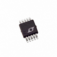
LTC3251EMSE Linear Technology, LTC3251EMSE Datasheet - Page 13

LTC3251EMSE
Manufacturer Part Number
LTC3251EMSE
Description
IC CONV DC/DC SDOWN HIEFF 10MSOP
Manufacturer
Linear Technology
Type
Step-Down (Buck), Switched Capacitor (Charge Pump)r
Datasheet
1.LTC3251EMSEPBF.pdf
(16 pages)
Specifications of LTC3251EMSE
Internal Switch(s)
Yes
Synchronous Rectifier
No
Number Of Outputs
1
Voltage - Output
0.9 ~ 1.6 V
Current - Output
500mA
Frequency - Switching
1MHz ~ 1.6MHz
Voltage - Input
2.7 ~ 5.5 V
Operating Temperature
-40°C ~ 85°C
Mounting Type
Surface Mount
Package / Case
10-MSOP Exposed Pad, 10-HMSOP, 10-eMSOP
Lead Free Status / RoHS Status
Contains lead / RoHS non-compliant
Power - Output
-
Other names
LTC3251EMS
LTC3251EMS
LTC3251EMS
Available stocks
Company
Part Number
Manufacturer
Quantity
Price
Company:
Part Number:
LTC3251EMSE
Manufacturer:
LT
Quantity:
10 000
Part Number:
LTC3251EMSE
Manufacturer:
LINEAR/凌特
Quantity:
20 000
Company:
Part Number:
LTC3251EMSE#PBF
Manufacturer:
LINEAR
Quantity:
429
Part Number:
LTC3251EMSE#TRPBF
Manufacturer:
LT/凌特
Quantity:
20 000
Part Number:
LTC3251EMSE-1.2
Manufacturer:
LINEAR/凌特
Quantity:
20 000
Company:
Part Number:
LTC3251EMSE-1.5
Manufacturer:
LT
Quantity:
10 000
Part Number:
LTC3251EMSE-1.5
Manufacturer:
LINEAR/凌特
Quantity:
20 000
OPERATIO
At moderate to high output power the switching losses
and quiescent current of the LTC3251 family is negligible
and the expression above is valid. For example with V
3.6V, I
measured efficiency is 81% which is in close agreement
with the theoretical 83.3% calculation.
Programming the LTC3251 Output Voltage (FB Pin)
The LTC3251 is programmed to an arbitrary output volt-
age via an external resistive divider. Figure 7 shows the
required voltage divider connection. The voltage divider
ratio is given by the expression:
Typical values for total voltage divider resistance can
range from several kΩs up to 1MΩ.
The user may want to consider load regulation when
setting the desired output voltage. The closed loop output
impedance of the LTC3251 is approximately:
R
R
A
B
R
O
OUT
=
≅
V
0 8
OUT
.
LTC3251
0 045
= 200mA and V
Figure 7. Programming the LTC3251
.
V
V
GND
OUT
–
FB
1
Ω
U
•
V
0 8
(Refer to Block Diagram)
OUT
.
C
A
V
R
R
A
B
OUT
regulating to 1.5V the
3251 F07
C
OUT
V
0.8V
OUT
( )
1 +
R
R
A
B
IN
=
For a 1.5V output, R
output change for a 500mA load current step. Thus, the
user may want to target an unloaded output voltage
slightly higher than desired to compensate for the output
load conditions. The output may be programmed for
regulation voltages of 0.9V to 1.6V.
Since the LTC3251 employs a 2-to-1 charge pump archi-
tecture, it is not possible to achieve output voltages
greater than half the available input voltage. The minimum
V
the following equation:
The compensation capacitor (C
act the pole caused by the large valued resistors R
and the input capacitance of the FB pin. For best results, C
should be 5pF for all R
omitted if both R
Disabling Spread Spectrum Operation on the
LTC3251-1.2/LTC3251-1.5 (MODE Pin)
Spread spectrum operation can be disabled by driving
MODE high. When Mode is high, switching takes place at
the maximum operating frequency (typ 1.6MHz). The
advantage of spread spectrum operation is that it reduces
the peak noise at and above the operating frequency at the
expense of a slightly increased noise floor and slightly
increased low frequency ripple caused by the converter
compensating for the changing operating frequency. Us-
ers who do not need the peak noise reduction gained by
using spread spectrum may wish to disable spread spec-
trum, thus improving the low frequency input/output
ripple.
IN
V
supply required for regulation can be determined by
IN(MIN)
LTC3251-1.2/LTC3251-1.5
≥ 2 • (V
A
and R
OUT(MIN)
O
is 0.085Ω, which produces a 40mV
A
or R
B
are less than 10k.
B
+ I
greater than 10k and can be
OUT
A
) is necessary to counter-
• R
OL
LTC3251/
)
A
13
and R
32511215fb
B
A
,


