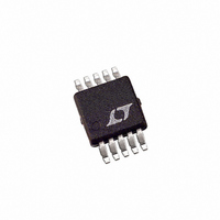
LTC3251EMSE Linear Technology, LTC3251EMSE Datasheet - Page 10

LTC3251EMSE
Manufacturer Part Number
LTC3251EMSE
Description
IC CONV DC/DC SDOWN HIEFF 10MSOP
Manufacturer
Linear Technology
Type
Step-Down (Buck), Switched Capacitor (Charge Pump)r
Datasheet
1.LTC3251EMSEPBF.pdf
(16 pages)
Specifications of LTC3251EMSE
Internal Switch(s)
Yes
Synchronous Rectifier
No
Number Of Outputs
1
Voltage - Output
0.9 ~ 1.6 V
Current - Output
500mA
Frequency - Switching
1MHz ~ 1.6MHz
Voltage - Input
2.7 ~ 5.5 V
Operating Temperature
-40°C ~ 85°C
Mounting Type
Surface Mount
Package / Case
10-MSOP Exposed Pad, 10-HMSOP, 10-eMSOP
Lead Free Status / RoHS Status
Contains lead / RoHS non-compliant
Power - Output
-
Other names
LTC3251EMS
LTC3251EMS
LTC3251EMS
Available stocks
Company
Part Number
Manufacturer
Quantity
Price
Company:
Part Number:
LTC3251EMSE
Manufacturer:
LT
Quantity:
10 000
Part Number:
LTC3251EMSE
Manufacturer:
LINEAR/凌特
Quantity:
20 000
Company:
Part Number:
LTC3251EMSE#PBF
Manufacturer:
LINEAR
Quantity:
429
Part Number:
LTC3251EMSE#TRPBF
Manufacturer:
LT/凌特
Quantity:
20 000
Part Number:
LTC3251EMSE-1.2
Manufacturer:
LINEAR/凌特
Quantity:
20 000
Company:
Part Number:
LTC3251EMSE-1.5
Manufacturer:
LT
Quantity:
10 000
Part Number:
LTC3251EMSE-1.5
Manufacturer:
LINEAR/凌特
Quantity:
20 000
OPERATIO
LTC3251/
LTC3251-1.2/LTC3251-1.5
capacitor selection, etc.), the part’s burst current is set by
the burst threshold and hysteresis. This means that the
V
and is typically 15mV with a 10µF output capacitor.
Ultralow Current Super Burst Mode Operation
To further optimize the supply current for low output
current requirements, a Super Burst mode operaton is
included in the LTC3251 family of parts. This mode is very
similar to Burst Mode operation, but much of the internal
circuitry and switch is shut down to further reduce supply
current. In Super Burst mode operation an internal hyster-
etic comparator is used to enable/disable charge transfer.
The hysteresis of the comparator and the amount of
current deliverable to the output are limited to keep output
ripple low. The V
operation is typically 35mV with a 10µF output capacitor.
The LTC3251 family can deliver 40mA of current in Super
Burst mode operation but does not switch to continuous
mode. The MODE pin of the LTC3251-1.2 and LTC3251-
1.5 has no effect on operation in super-burst mode.
V
The style and value of capacitors used with the LTC3251
family determine several important parameters such as
regulator control loop stability, output ripple and charge
pump strength.
The dual phase nature of the LTC3251 family minimizes
output noise significantly but not completely. What small
ripple that does exist is controlled by the value of C
directly. Increasing the size of C
reduce the output ripple. The ESR (equivalent series
resistance) of C
noise. When a part switches between clock phases there
is a period where all switches are turned off. This “blanking
period” shows up as a spike at the output and is a direct
function of the output current times the ESR value. To
reduce output noise and ripple, it is suggested that a low
ESR (<0.08Ω) ceramic capacitor be used for C
lum and aluminum capacitors are not recommended be-
cause of their high ESR.
Both the style and value of C
stability of the LTC3251 family. As shown in the Block
10
OUT
OUT
ripple voltage in Burst Mode operation will be fixed
Capacitor Selection
OUT
OUT
U
plays the dominant role in output
ripple voltage in Super Burst mode
(Refer to Block Diagram)
OUT
can significantly affect the
OUT
will proportionately
OUT
. Tanta-
OUT
Diagram, the LTC3251 family uses a control loop to adjust
the strength of the charge pump to match the current
required at the output. The error signal of this loop is
stored directly on the output charge storage capacitor.
Thus the charge storage capacitor also serves to form the
dominant pole for the control loop. The desired output
voltage also affects stability. As the divider ratio (R
drops, the effective closed-loop gain increases, thus re-
quiring a larger output capacitor for stability. Figure 3
shows the suggested output capacitor for optimal tran-
sient response. The value of the output capacitance should
not drop below the minimum capacitance line to prevent
excessive ringing or instability. (see Ceramic Capacitor
Selection Guidelines section).
Likewise excessive ESR on the output capacitor will tend
to degrade the loop stability. The closed loop output
impedance of the LTC3251 is approximately:
For example, with the output programmed to 1.5V, the R
is 0.085Ω, which produces a 40mV output change for a
500mA load current step. For stability and good load
transient response, it is important for the output capacitor
to have 0.08Ω or less of ESR. Ceramic capacitors typically
have exceptional ESR, and combined with a tight board
layout, should yield excellent stability and load transient
performance.
R
O
≅
0 045
.
10
16
15
14
13
12
11
9
8
7
6
5
4
0.9
Ω
1.0
•
V
0 8
OUT
.
1.1
MINIMUM CAPACITANCE
V
Figure 3
1.2
V
OPTIMUM CAPACITANCE
OUT
1.3
(V)
1.4
1.5
3251 F03
1.6
32511215fb
A
/R
B
O
)


