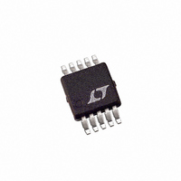
LTC3251EMSE Linear Technology, LTC3251EMSE Datasheet

LTC3251EMSE
Specifications of LTC3251EMSE
LTC3251EMS
Available stocks
Related parts for LTC3251EMSE
LTC3251EMSE Summary of contents
Page 1
... The parts are short-circuit and overtempera- ture protected, and are available in a thermally enhanced 10-pin MSOP package. , LT, LTC and LTM are registered trademarks of Linear Technology Corporation. Burst Mode is a registered trademark of Linear Technology Corporation. Super Burst is a trademark of Linear Technology Corporation. ...
Page 2
... MD1 IN 0mA ≤ I ≤ 500mA, Referred to FB Pin OUT TOP VIEW ORDER PART 10 MODE NUMBER 9 MD1 + LTC3251EMSE-1 OUT – LTC3251EMSE-1.5 MSE PACKAGE MSE PART MARKING LTAGM = 40°C/W, θ LTABE = 10°C 1µ 10µF, IN OUT MIN TYP MAX ● 2.7 ● 5.5 ● ● ...
Page 3
ELECTRICAL CHARACTERISTICS temperature range, otherwise specifications are for LTC3251-1.2V or LTC3251-1.5, V MODE PARAMETER Line Regulation (LTC3251) Spread Spectrum Frequency Range Spread Spectrum Disabled Frequency MD0, MD1 Input High Voltage MD0, MD1 Input Low Voltage ...
Page 4
LTC3251/ LTC3251-1.2/LTC3251-1 TYPICAL PERFOR A CE CHARACTERISTICS No Load Supply Current vs Supply Voltage (Super Burst Mode Operation 85°C 25°C 10 –40° 2.7 4.2 4.7 5.2 3.2 3.7 ...
Page 5
W U TYPICAL PERFOR A CE CHARACTERISTICS MD0/MD1 Input Threshold Voltage vs Supply Voltage 1.2 1.1 1.0 –40°C 0.9 25°C 0.8 85°C 0.7 0.6 0.5 0.4 2.7 4.2 3.2 3.7 V (V) IN Output Transient Response (Continuous Mode) 450mA I ...
Page 6
LTC3251/ LTC3251-1.2/LTC3251-1 CTIO S MD0 (Pin 1)/MD1 (Pin 9): Switching Mode Input Pins. The Mode input pins are used to set the operating mode of the LTC3251. The modes of operation are: MD1 MD0 OPERATING ...
Page 7
W SI PLIFIED BLOCK DIAGRA OVERTEMP BURST DETECT CIRCUIT LTC3251-1.2/LTC3251-1.5 W LTC3251-1.2/ LTC3251-1.5 ONLY MD0 MD1 MODE SWITCH CONTROL SPREAD SPECTRUM AND SOFT-START OSCILLATOR CHARGE PUMP 1 CHARGE PUMP 2 – + GND 5 ...
Page 8
LTC3251/ LTC3251-1.2/LTC3251-1.5 U OPERATIO (Refer to Block Diagram) The LTC3251 family of parts use a dual phase switched capacitor charge pump to step down V output voltage. Regulation is achieved by sensing the output voltage through an external resistor divider ...
Page 9
U OPERATIO (Refer to Block Diagram) 4.7µ 10µF FB COMP GND Figure 1a. Conventional Buck Switching Converter –40 –50 –60 –70 –80 –90 START FREQ: 100kHz RBW: 10kHz STOP FREQ: 30MHz Figure 1b. Conventional Buck Converter ...
Page 10
LTC3251/ LTC3251-1.2/LTC3251-1.5 U OPERATIO (Refer to Block Diagram) capacitor selection, etc.), the part’s burst current is set by the burst threshold and hysteresis. This means that the V ripple voltage in Burst Mode operation will be fixed OUT and is ...
Page 11
U OPERATIO (Refer to Block Diagram) Further output noise reduction can be achieved by filtering the LTC3251 output through a very small series inductor as shown in Figure 4. A 10nH inductor will reject the fast output transients caused by ...
Page 12
LTC3251/ LTC3251-1.2/LTC3251-1.5 U OPERATIO (Refer to Block Diagram) temperature range, the 1µF, 10V, X5R or X7R will provide more capacitance than the 4.7µF, 10V, Y5V. The capacitor manufacturer’s data sheet should be consulted to deter- mine what value of capacitor ...
Page 13
U OPERATIO (Refer to Block Diagram) At moderate to high output power the switching losses and quiescent current of the LTC3251 family is negligible and the expression above is valid. For example with V 3.6V 200mA and V ...
Page 14
LTC3251/ LTC3251-1.2/LTC3251-1.5 U TYPICAL APPLICATIO S 0.9V Output Continuous/Burst Mode Operation with Shutdown 1-CELL Li-Ion OR 3-CELL NiMH 14 OFF MD0 MD1 LTC3251 OUT 1µ 1µF ...
Page 15
... LEAD COPLANARITY (BOTTOM OF LEADS AFTER FORMING) SHALL BE 0.102mm (.004") MAX Information furnished by Linear Technology Corporation is believed to be accurate and reliable. However, no responsibility is assumed for its use. Linear Technology Corporation makes no represen- tation that the interconnection of its circuits as described herein will not infringe on existing patent rights. ...
Page 16
... Regulated Output, IN OUT : 3.1V to 5.5V 1.5V, Regulated Output, IN OUT : 2.7V to 5.5V 0.9V to 1.6V, IN OUT : 0.8V, OUT(MIN) : 0.8V, OUT(MIN) : 0.6V, OUT(MIN) : 0.8V, OUT(MIN) : 0.8V, OUT(MIN) : 2.5V to 5.5V, OUT : 2.4V to 5.25V, OUT LT 0306 REV B • PRINTED IN USA © LINEAR TECHNOLOGY CORPORATION 2003 32511215fb ...


