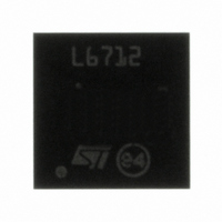
L6712QTR STMicroelectronics, L6712QTR Datasheet - Page 9

L6712QTR
Manufacturer Part Number
L6712QTR
Description
IC CTRLR DC/DC 2PH SYNC 36VFQFPN
Manufacturer
STMicroelectronics
Type
Step-Down (Buck)r
Datasheet
1.L6712AQTR.pdf
(29 pages)
Specifications of L6712QTR
Internal Switch(s)
No
Synchronous Rectifier
Yes
Number Of Outputs
2
Voltage - Output
0.9 ~ 3.3 V
Current - Output
2A
Frequency - Switching
150kHz
Voltage - Input
12V
Operating Temperature
0°C ~ 70°C
Mounting Type
Surface Mount
Package / Case
36-VFQFN, 36-VFQFPN
Power - Output
3.5W
Operating Temperature Range
- 40 C to + 125 C
Mounting Style
SMD/SMT
Lead Free Status / RoHS Status
Lead free / RoHS Compliant
Other names
497-4219-2
Available stocks
Company
Part Number
Manufacturer
Quantity
Price
Figure 5. R
3.2 DIGITAL TO ANALOG CONVERTER AND REFERENCE
The built-in digital to analog converter allows the adjustment of the output voltage from 0.900V to 3.300V
as shown in Figure 6. Different voltages can be reached simply changing the Remote Amplifier Gain that
acts as a resistor divider (See relevant section).
The internal reference is trimmed during production process to have an output voltage accuracy of ±0.9%
and a zero temperature coefficient around 70°C including also error amplifier offset compensation. It is
programmed through the voltage identification (VID) pins. These are inputs of an internal DAC that is re-
alized by means of a series of resistors providing a partition of the internal voltage reference. The VID code
drives a multiplexer that select a voltage on a precise point of the divider (see Figure 6). The DAC output
is delivered to an amplifier obtaining the V
Internal pull-ups are provided (realized with a 5µA current generator up to 3V typ.); in this way, to program
a logic "1" it is enough to leave the pin floating, while to program a logic "0" it is enough to short the pin to
SGND.
The device offers a bi-directional pin REF_IN/OUT: the internal reference used for the regulation is usually
available on this pin with 3mA of maximum current capability except when VID code 111 is programmed;
in this case the device accepts an external reference through the REF_IN/OUT pin and regulates on it.
When external reference is used, it must range from 0.800V up to 3.300V to assure proper functionality of
the device.
Figure 6 shows a block schematic of how the Reference for the regulation is managed when internal or
external reference is used.
The voltage identification (VID) pin configuration or the external reference provided also sets the power-
good thresholds (PGOOD) and the Over/Under voltage protection (OVP/UVP) thresholds.
14000
12000
10000
8000
6000
4000
2000
0
OSC
25
vs. Switching Frequency
50
Frequency (kHz)
75
100
125
PROG
150
voltage reference (i.e. the set-point of the error amplifier).
800
700
600
500
400
300
200
100
0
150
250
Frequency (kHz)
350
450
L6712A L6712
550
650
9/29


