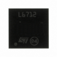
L6712QTR STMicroelectronics, L6712QTR Datasheet - Page 25

L6712QTR
Manufacturer Part Number
L6712QTR
Description
IC CTRLR DC/DC 2PH SYNC 36VFQFPN
Manufacturer
STMicroelectronics
Type
Step-Down (Buck)r
Datasheet
1.L6712AQTR.pdf
(29 pages)
Specifications of L6712QTR
Internal Switch(s)
No
Synchronous Rectifier
Yes
Number Of Outputs
2
Voltage - Output
0.9 ~ 3.3 V
Current - Output
2A
Frequency - Switching
150kHz
Voltage - Input
12V
Operating Temperature
0°C ~ 70°C
Mounting Type
Surface Mount
Package / Case
36-VFQFN, 36-VFQFPN
Power - Output
3.5W
Operating Temperature Range
- 40 C to + 125 C
Mounting Style
SMD/SMT
Lead Free Status / RoHS Status
Lead free / RoHS Compliant
Other names
497-4219-2
Available stocks
Company
Part Number
Manufacturer
Quantity
Price
erance.
Current Reading: The Rg resistor has to be placed as close as possible to the ISENx and PGNDSx pins
in order to limit the noise injection into the device. The PCB traces connecting these resistors to the read-
ing point must be routed as parallel traces in order to avoid the pick-up of any noise. It's also important to
avoid any offset in the measurement and to get a better precision, to connect the traces as close as pos-
sible to the sensing elements, dedicated current sense resistor or low side mosfet R
Moreover, when using the low side mosfet R
connected to the PHASEx pin. DO NOT CONNECT THE PINS TOGETHER AND THEN TO THE HS
SOURCE! The device won't work properly because of the noise generated by the return of the high side
driver. In this case route two separate nets: connect the PHASEx pin to the HS Source (route together
with HGATEx) with a wide net (30 mils) and the ISENx pin to the LS Drain (route together with PGNDSx).
Moreover, the PGNDSx pin is always connected, through the Rg resistor, to the PGND: DO NOT CON-
NECT DIRECTLY TO THE PGND! In this case the device won't work properly. Route anyway to the LS
mosfet source (together with ISENx net).
Right and wrong connections are reported in Figure 21.
Symmetrical layout is also suggested to avoid any unbalance between the two phases of the converter.
Figure 21. PCB layout connections for sense nets.
VIA to GND plane
Wrong (left) and correct (right) connections for the current reading sensing nets.
NOT CORRECT
To PHASE
connection
dsON
as current sense element, the ISENx pin is practically
CORRECT
dsON
L6712A L6712
To LS Drain
and Source
To HS Gate
and Source
.
25/29


