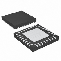
MAX17004ETJ+ Maxim Integrated Products, MAX17004ETJ+ Datasheet - Page 13

MAX17004ETJ+
Manufacturer Part Number
MAX17004ETJ+
Description
IC PS CTRLR FOR NOTEBOOKS 32TQFN
Manufacturer
Maxim Integrated Products
Datasheet
1.MAX17003ETJ.pdf
(36 pages)
Specifications of MAX17004ETJ+
Applications
Controller, Notebook Computers
Voltage - Input
6 ~ 26 V
Number Of Outputs
4
Voltage - Output
3.3V, 5V, 2 ~ 5.5 V
Operating Temperature
-40°C ~ 85°C
Mounting Type
Surface Mount
Package / Case
32-TQFN Exposed Pad
Lead Free Status / RoHS Status
Lead free / RoHS Compliant
PIN
10
11
12
13
14
1
2
3
4
5
6
7
8
9
Supply Controllers for Notebook Computers
DSCHG5
NAME
SHDN
DRVA
CSH5
FSEL
CSL5
GND
ONA
ON3
ON5
SKIP
ILIM
REF
FB5
High-Efficiency, Quad-Output, Main Power-
______________________________________________________________________________________
Auxiliary LDO Enable Input. When ONA is pulled low, OUTA is high impedance and the secondary feedback
control is disabled. When ONA is driven high, the controller enables the auxiliary LDO.
Auxiliary LDO Transistor Base Driver. Connect DRVA to the base of a pnp power transistor. Add a 680Ω
pullup resistor between the base and emitter.
Peak Current-Limit Threshold Adjustment. The current-limit threshold defaults to 50mV if ILIM is pulled up to
LDO5. In adjustable mode, the current-limit threshold across CSH_ and CSL_ is precisely 1/10th the voltage
seen at ILIM over a 0.5V to 2.0V range. The logic threshold for switchover to the 50mV default value is
approximately V
Shutdown Control Input. The device enters its 8µA supply-current shutdown mode if V
SHDN input falling-edge trip level and does not restart until V
edge trip level. Connect SHDN to V
resistive voltage-divider to implement a programmable undervoltage lockout.
3.3V SMPS Enable Input. Driving ON3 high enables the 3.3V SMPS, while pulling ON3 low disables the 3.3V
SMPS. If ON3 is connected to REF, the 3.3V SMPS starts after the 5V SMPS reaches regulation (delayed
start). Drive ON3 below the clear fault level to reset the fault latch.
5V SMPS Enable Input. Driving ON5 high enables the 5V SMPS, while pulling ON5 low disables the 5V
SMPS. If ON5 is connected to REF, the 5V SMPS starts after the 3.3V SMPS reaches regulation (delayed
start). Drive ON5 below the clear fault level to reset the fault latch.
2.0V Reference Voltage Output. Bypass REF to analog ground with a 0.1µF or greater ceramic capacitor.
The reference sources up to 50µA for external loads. Loading REF degrades output-voltage accuracy
according to the REF load-regulation error. The reference shuts down when the system pulls SHDN low.
Analog Ground. Connect the exposed backside pad to GND.
Frequency Select Input. This three-level logic input sets the controllers’ switching frequency. Connect to
LDO5, REF, or GND to select the following typical switching frequencies:
LDO5 = 500kHz, REF = 300kHz, GND = 200kHz.
Pulse-Skipping Control Input. Connect to LDO5 for low-noise, forced-PWM operation. Connect to REF for
automatic, low-noise, pulse-skipping operation at light loads. Connect to GND for automatic, high-efficiency,
pulse-skipping operation at light loads. Startup is always in the low-noise, pulse-skipping mode (i.e., same
as SKIP = REF setting), regardless of the SKIP setting. The SKIP setting takes effect once the respective
SMPS is in regulation.
Feedback Input for the 5V SMPS. Connect to LDO5 for the preset 5V output. In adjustable mode, FB5
regulates to 2V.
P osi ti ve C ur r ent- S ense Inp ut for the 5V S M P S . C onnect to the p osi ti ve ter m i nal of the cur r ent- sense el em ent.
Fi g ur e 7 d escr i b es tw o d i ffer ent cur r ent- sensi ng op ti ons— usi ng accur ate sense r esi stor s or l ossl ess i nd uctor
D C R sensi ng .
Output-Sense and Negative Current-Sense Input for the 5V SMPS. When using the internal preset 5V
feedback-divider (FB5 = LDO5), the controller uses CSL5 to sense the output voltage. Connect to the
negative terminal of the current-sense element. CSL5 also serves as the bootstrap input for LDO5. For the
MAX17003, place a Schottky diode from CSL5 to GND to prevent CSL5 from going below -7V.
Open-Drain Discharge Input for the 5V SMPS. DSCHG5 is pulled low when ON5 is low, discharging the
SMPS5 output. DSCHG5 is also low under fault conditions.
Connect a resistor from DSCHG5 to the SMPS5 output. Limit the peak discharge current to less than 100mA:
where R
DSCHG5(MIN)
LDO5
is 5Ω, taken from the Electrical Characteristics.
- 1V.
R
DIS
5
≥
100
IN
V
OUT
for automatic startup. SHDN can be connected to V
mA
5
−
R
DSCHG MIN
FUNCTION
5
(
)
SHDN
is greater than the SHDN input rising-
Pin Description
SHDN
IN
through a
is less than the
13


