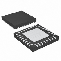
MAX1518ETJ+ Maxim Integrated Products, MAX1518ETJ+ Datasheet - Page 24

MAX1518ETJ+
Manufacturer Part Number
MAX1518ETJ+
Description
IC DC/DC CONV W/OP AMP 32-TQFN
Manufacturer
Maxim Integrated Products
Datasheet
1.MAX1517ETJ.pdf
(26 pages)
Specifications of MAX1518ETJ+
Applications
Converter, TFT, LCD
Voltage - Input
2.6 ~ 5.5 V
Number Of Outputs
1
Voltage - Output
2.6 ~ 13 V
Operating Temperature
-40°C ~ 100°C
Mounting Type
Surface Mount
Package / Case
32-TQFN Exposed Pad
Lead Free Status / RoHS Status
Lead free / RoHS Compliant
TFT-LCD DC-DC Converters with
Operational Amplifiers
An IC’s maximum power dissipation depends on the
thermal resistance from the die to the ambient environ-
ment and the ambient temperature. The thermal resis-
tance depends on the IC package, PC board copper
area, other thermal mass, and airflow.
The MAX1516/MAX1517/MAX1518, with their exposed
backside pad soldered to 1in
can dissipate about 1.7W into +70°C still air. More PC
board copper, cooler ambient air, and more airflow
increase the possible dissipation, while less copper or
warmer air decreases the IC’s dissipation capability.
The major components of power dissipation are the
power dissipated in the step-up regulator and the
power dissipated by the operational amplifiers.
The largest portions of power dissipation in the step-up
regulator are the internal MOSFET, the inductor, and the
output diode. If the step-up regulator has 90% efficiency,
about 3% to 5% of the power is lost in the internal
MOSFET, about 3% to 4% in the inductor, and about 1%
in the output diode. The remaining 1% to 3% is distrib-
uted among the input and output capacitors and the PC
board traces. If the input power is about 5W, the power
lost in the internal MOSFET is about 150mW to 250mW.
The power dissipated in the operational amplifiers
depends on their output current, the output voltage,
and the supply voltage:
where I
the operational amplifier, and I
current that the operational amplifier sinks.
In a typical case where the supply voltage is 13V and
the output voltage is 6V with an output source current
of 30mA, the power dissipated is 180mV.
Careful PC board layout is important for proper opera-
tion. Use the following guidelines for good PC board
layout:
• Minimize the area of high-current loops by placing
24
the inductor, the output diode, and the output
capacitors near the input capacitors and near the
LX and PGND pins. The high-current input loop
goes from the positive terminal of the input capacitor
PD
PD
______________________________________________________________________________________
SOURCE
SINK
OUT_(SOURCE)
=
I
OUT SINK
PC Board Layout and Grounding
Applications Information
=
I
OUT SOURCE
_(
_(
is the output current sourced by
)
×
V
OUT
OUT_(SINK)
2
)
Power Dissipation
Operational Amplifier
×
_
of PC board copper,
(
V
Step-Up Regulator
SUP
−
V
is the output
OUT
_
)
• Create a power-ground island (PGND) consisting of
• Place all feedback voltage-divider resistors as close
• Place the IN pin and REF pin bypass capacitors as
• Minimize the length and maximize the width of the
• Minimize the size of the LX node while keeping it
Refer to the MAX1518 evaluation kit for an example of
proper PC board layout.
TRANSISTOR COUNT: 4608
PROCESS: BiCMOS
to the inductor, to the IC’s LX pin, out of PGND, and
to the input capacitor’s negative terminal. The high-
current output loop is from the positive terminal of
the input capacitor to the inductor, to the output
diode (D1), and to the positive terminal of the output
capacitors, reconnecting between the output capac-
itor and input capacitor ground terminals. Connect
these loop components with short, wide connec-
tions. Avoid using vias in the high-current paths. If
vias are unavoidable, use many vias in parallel to
reduce resistance and inductance.
the input and output capacitor grounds, PGND pin,
and any charge-pump components. Connect all of
these together with short, wide traces or a small
ground plane. Maximizing the width of the power-
ground traces improves efficiency and reduces out-
put voltage ripple and noise spikes. Create an
analog ground plane (AGND) consisting of the
AGND pin, all the feedback-divider ground connec-
tions, the operational-amplifier divider ground con-
nections, the COMP and DEL capacitor ground
connections, and the device’s exposed backside
pad. Connect the AGND and PGND islands by con-
necting the PGND pin directly to the exposed back-
side pad. Make no other connections between these
separate ground planes.
to their respective feedback pins as possible. The
divider’s center trace should be kept short. Placing
the resistors far away causes their FB traces to
become antennas that can pick up switching noise.
Take care to avoid running any feedback trace near
LX or the switching nodes in the charge pumps.
close to the device as possible. The ground connec-
tion of the IN bypass capacitor should be connected
directly to the AGND pin with a wide trace.
traces between the output capacitors and the load
for best transient responses.
wide and short. Keep the LX node away from feed-
back nodes (FB, FBP, and FBN) and analog ground.
Use DC traces to shield if necessary.
Chip Information


