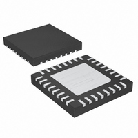
MAX1518ETJ+ Maxim Integrated Products, MAX1518ETJ+ Datasheet - Page 21

MAX1518ETJ+
Manufacturer Part Number
MAX1518ETJ+
Description
IC DC/DC CONV W/OP AMP 32-TQFN
Manufacturer
Maxim Integrated Products
Datasheet
1.MAX1517ETJ.pdf
(26 pages)
Specifications of MAX1518ETJ+
Applications
Converter, TFT, LCD
Voltage - Input
2.6 ~ 5.5 V
Number Of Outputs
1
Voltage - Output
2.6 ~ 13 V
Operating Temperature
-40°C ~ 100°C
Mounting Type
Surface Mount
Package / Case
32-TQFN Exposed Pad
Lead Free Status / RoHS Status
Lead free / RoHS Compliant
The number of negative charge-pump stages is given by:
where n
stages, V
output, V
is the forward-voltage drop of the charge-pump diode,
and V
ulator. Use V
The above equations are derived based on the
assumption that the first stage of the positive charge
pump is connected to V
negative charge pump is connected to ground.
Sometimes fractional stages are more desirable for bet-
ter efficiency. This can be done by connecting the first
stage to V
charge-pump stage is powered from V
above equations become:
Increasing the flying-capacitor (C
effective source impedance and increases the output-
current capability. Increasing the capacitance indefi-
Figure 8. Operation with Output Voltages >13V Using
Cascoded MOSFET
V
DROPOUT
IN
NEG
MAIN
GOFF
n
n
IN
POS
NEG
CONTROLLER
n
DROPOUT
STEP-UP
is the number of negative charge-pump
NEG
or another available supply. If the first
is the main step-up regulator output, V
MAX1516
MAX1517
MAX1518
is the dropout margin for the linear reg-
is the gate-off linear-regulator REG N
=
=
V
−
______________________________________________________________________________________
=
GON
V
−
GOFF
V
= 0.3V.
V
GOFF
V
MAIN
+
V
MAIN
MAIN
MAIN
V
+
DROPOUT
LX
V
+
DROPOUT
FB
PGND
− ×
− ×
and the first stage of the
V
− ×
2
DROPOUT
2
2
V
V
D
V
X
D
D
) value lowers the
Flying Capacitors
+
V
TFT-LCD DC-DC Converters with
+
IN
V
IN
IN
, then the
V
>13V
MAIN
D
nitely has a negligible effect on output-current capabili-
ty because the internal switch resistance and the diode
impedance place a lower limit on the source imped-
ance. A 0.1µF ceramic capacitor works well in most
low-current applications. The flying capacitor’s voltage
rating must exceed the following:
where n is the stage number in which the flying capaci-
tor appears, and V
main step-up regulator.
Increasing the output capacitance or decreasing the
ESR reduces the output ripple voltage and the peak-to-
peak transient voltage. With ceramic capacitors, the
output voltage ripple is dominated by the capacitance
value. Use the following equation to approximate the
required capacitor value:
where C
pump, I
pump, and V
output ripple.
Use low-cost silicon switching diodes with a current rat-
ing equal to or greater than two times the average
charge-pump input current. If it helps avoid an extra
stage, some or all of the diodes can be replaced with
Schottky diodes with an equivalent current rating.
Adjust the gate-on linear-regulator (REG P) output volt-
age by connecting a resistive voltage-divider from the
REG P output to AGND with the center tap connected
to FBP (Figure 1). Select the lower resistor of the divider
R5 in the range of 10kΩ to 30kΩ. Calculate the upper
resistor R4 with the following equation:
where V
Operational Amplifiers
FBP
LOAD_CP
OUT_CP
C
= 1.25V (typ).
RIPPLE_CP
OUT CP
is the output capacitor of the charge
R
_
Linear-Regulator Controllers
4
is the load current of the charge
V
MAIN
=
CX
Charge-Pump Output Capacitor
R
≥
Charge-Pump Rectifier Diodes
5
is the peak-to-peak value of the
2
> ×
×
f
n V
OSC
is the output voltage of the
V
V
Output-Voltage Selection
I
GON
LOAD CP
FBP
MAIN
V
RIPPLE CP
−
_
1
_
21


