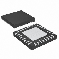
MAX1518ETJ+ Maxim Integrated Products, MAX1518ETJ+ Datasheet - Page 16

MAX1518ETJ+
Manufacturer Part Number
MAX1518ETJ+
Description
IC DC/DC CONV W/OP AMP 32-TQFN
Manufacturer
Maxim Integrated Products
Datasheet
1.MAX1517ETJ.pdf
(26 pages)
Specifications of MAX1518ETJ+
Applications
Converter, TFT, LCD
Voltage - Input
2.6 ~ 5.5 V
Number Of Outputs
1
Voltage - Output
2.6 ~ 13 V
Operating Temperature
-40°C ~ 100°C
Mounting Type
Surface Mount
Package / Case
32-TQFN Exposed Pad
Lead Free Status / RoHS Status
Lead free / RoHS Compliant
TFT-LCD DC-DC Converters with
Operational Amplifiers
Figure 4. Using Cascoded npn for Charge-Pump Output
Voltages >28V
The gate-off linear-regulator controller (REG N) is an
analog gain block with an open-drain p-channel output.
It drives an external npn pass transistor with a 6.8kΩ
base-to-emitter resistor (Figure 1). Its guaranteed base-
drive source current is at least 1mA. The regulator
including Q2 in Figure 1 uses a 0.47µF ceramic output
capacitor and is designed to deliver 50mA at -8V. Other
output voltages and currents are possible with the proper
pass transistor and output capacitor (see the Pass-
Transistor Selection and Stability Requirements sections).
REG N is typically used to provide the TFT-LCD gate
drivers’ gate-off voltage. A negative voltage can be
produced using a charge-pump circuit as shown in
Figure 1. REG N is enabled after the voltage on REF
exceeds 1.0V. Each time it is enabled, the control goes
through a soft-start routine that ramps down its internal
reference DAC from V
The MAX1518 has five operational amplifiers, the
MAX1517 has three operational amplifiers, and the
MAX1516 has one operational amplifier. The operational
amplifiers are typically used to drive the LCD backplane
(VCOM) or the gamma-correction divider string. They
feature ±150mA output short-circuit current, 13V/µs slew
rate, and 12MHz bandwidth. The rail-to-rail input and
output capability maximizes system flexibility.
16
Gate-Off Linear-Regulator Controller, REG N
______________________________________________________________________________________
MAX1516
MAX1517
MAX1518
DRVP
FBP
NPN CASCODE
TRANSISTOR
V
REF
MAIN
to 250mV in 128 steps.
Operational Amplifiers
FROM CHARGE-PUMP
OUTPUT
PNP PASS
TRANSISTOR
V
GON
The operational amplifiers limit short-circuit current to
approximately ±150mA if the output is directly shorted to
SUP or to BGND. If the short-circuit condition persists, the
junction temperature of the IC rises until it reaches the
thermal-shutdown threshold (+160°C typ). Once the junc-
tion temperature reaches the thermal-shutdown threshold,
an internal thermal sensor immediately sets the thermal
fault latch, shutting off all the IC’s outputs. The device
remains inactive until the input voltage is cycled.
The operational amplifiers are typically used to drive
the LCD backplane (VCOM) or the gamma-correction
divider string. The LCD backplane consists of a distrib-
uted series capacitance and resistance, a load that can
be easily driven by the operational amplifier. However,
if the operational amplifier is used in an application with
a pure capacitive load, steps must be taken to ensure
stable operation.
As the operational amplifier’s capacitive load increases,
the amplifier’s bandwidth decreases and gain peaking
increases. A 5Ω to 50Ω small resistor placed between
OUT_ and the capacitive load reduces peaking but also
reduces the gain. An alternative method of reducing
peaking is to place a series RC network (snubber) in par-
allel with the capacitive load. The RC network does not
continuously load the output or reduce the gain. Typical
values of the resistor are between 100Ω and 200Ω, and
the typical value of the capacitor is 10nF.
Figure 5. The linear regulator controls the intermediate charge-
pump stage.
MAX1516
MAX1517
MAX1518
DRVP
FBP
0.1µF
6.8kΩ
0.47µF
Driving Pure Capacitive Load
Q1
Short-Circuit Current Limit
0.1µF
10.0kΩ
267kΩ
1%
1%
0.22µF
LX
V
13V
V
MAIN
35V
GON


