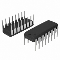
NCP1395APG ON Semiconductor, NCP1395APG Datasheet - Page 6

NCP1395APG
Manufacturer Part Number
NCP1395APG
Description
IC CTRLR PWM OVP 16DIP
Manufacturer
ON Semiconductor
Datasheet
1.NCP1395APG.pdf
(27 pages)
Specifications of NCP1395APG
Pwm Type
Voltage Mode
Number Of Outputs
1
Frequency - Max
1MHz
Duty Cycle
52%
Voltage - Supply
10.3 V ~ 20 V
Buck
No
Boost
No
Flyback
No
Inverting
No
Doubler
No
Divider
No
Cuk
No
Isolated
No
Operating Temperature
-40°C ~ 125°C
Package / Case
16-DIP (0.300", 7.62mm)
Frequency-max
1MHz
Switching Frequency
50 KHz to 1 MHz
Mounting Style
Through Hole
Duty Cycle (max)
52 %
Input Voltage
11V
Frequency
1MHz
Supply Voltage Range
20V
Digital Ic Case Style
DIP
No. Of Pins
16
Operating Temperature Range
-40°C To +125°C
Svhc
No SVHC (15-Dec-2010)
Base Number
1395
Rohs Compliant
Yes
Lead Free Status / RoHS Status
Lead free / RoHS Compliant
3. Room temperature only, please look at characterization data for evolution versus junction temperature.
Turn−On Threshold Level, V
Turn−On Threshold Level, V
Minimum Operating Voltage after Turn−On
Minimum Hysteresis between VCC
Minimum Hysteresis between VCC
Startup Current, V
V
Internal IC Consumption, No Output Load on Pins 11/12, Fsw = 300 kHz
Internal IC consumption, 100 pF output load on pin 11 / 12, Fsw = 300 kHz
Consumption in fault mode (All drivers disabled, Vcc > VCC
Minimum Switching Frequency, Rt = 120 kW on Pin 1, Vpin 5 = 0 V,
DT = 300 ns
Maximum Switching Frequency, Rfmax = 22 kW on Pin 2, Vpin 5 >
6.0 V, DT = 300 ns − T
Feedback Pin Swing above which Df = 0
VCO V
Operating Duty Cycle
Reference Voltage for all Current Generations (Fosc, DT)
Delay before any Driver Restart in Fault Mode
Internal Pulldown Resistor
OTA Internal Offset Voltage
Voltage on Pin 5 below which the FB Level has no VCO Action
Voltage on Pin 5 below which the Controller Considers a Fault
Input Bias Current
DC Transconductance Gain
Gain Product Bandwidth, Rload = 5.0 kW
Output Voltage Rise Time @ CL = 100 pF, 10−90% of Output Signal
Output Voltage Fall−Time @ CL = 100 pF, 10−90% of Output Signal
Source Resistance
Sink Resistance
Deadtime with R
Maximum Deadtime with R
Minimum Deadtime, R
ELECTRICAL CHARACTERISTICS (For typical values T
V
SUPPLY SECTION
VOLTAGE CONTROL OSCILLATOR (VCO)
FEEDBACK SECTION
DRIVE OUTPUT
CC
CC
Level at which the Internal Logic gets Reset
= 11 V, unless otherwise noted.)
CC
Rejection, DV
DT
CC
= 127 kW from Pin 3 to GND
< VCC
DT
j
= 25°C (Note 3)
CC
= 30 kW from Pin 3 to GND
DT
= 1.0 V, in Percentage of Fsw
CC
CC
ON
Characteristic
= 540 kW from Pin 3 to GND
Going Up – A Version
Going Up – B Version
ON
ON
and VCC
and VCC
(min)
(min)
− A Version
− B Version
j
http://onsemi.com
= 25°C, for min/max values T
(min)
)
6
11−10
11−10
11−10
11−10
11−10
1, 3
Pin
12
12
12
12
12
12
12
12
12
12
16
16
15
15
1
2
5
−
−
5
5
5
3
3
3
T_dead−max
T_dead−min
j
= −40°C to +125°C, Max T
VREF_FB
VCC
VCC
Fsw max
Vfb_fault
VhysteA
VhysteB
Fsw min
Symbol
VCC
VCC
Istartup
T_dead
Vfb_off
FBSW
PSRR
OTAG
VREF
ICC1
ICC2
ICC3
GBW
IBias
Tdel
R
R
Rfb
DC
T
T
OH
OL
(min)
reset
r
f
ON
ON
2.325
12.3
48.5
1.86
Min
270
9.3
8.3
0.9
48
20
30
−
−
−
−
−
−
−
−
−
−
−
−
−
−
−
−
−
−
−
−
13.3
10.3
Typ
250
300
150
9.3
3.0
1.0
5.9
1.6
2.3
1.3
1.0
6.0
0.2
2.0
2.5
1.3
0.6
1.0
1.0
J
50
50
20
20
20
20
60
60
−
−
= 150°C,
2.675
Max
14.3
11.3
10.3
51.5
1.11
2.14
300
100
120
130
390
52
−
−
−
−
−
−
−
−
−
−
−
−
−
−
−
−
−
−
Unit
MHz
MHz
%/V
kHz
mA
mA
mA
kW
mA
nA
mS
ms
ns
ns
ns
ms
ns
%
W
W
V
V
V
V
V
V
V
V
V
V
V


