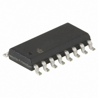
ISL6721ABZ Intersil, ISL6721ABZ Datasheet - Page 16

ISL6721ABZ
Manufacturer Part Number
ISL6721ABZ
Description
IC CTRLR PWM SGL ENDED 16-SOIC
Manufacturer
Intersil
Datasheet
1.ISL6721ABZ.pdf
(22 pages)
Specifications of ISL6721ABZ
Pwm Type
Current Mode
Number Of Outputs
1
Frequency - Max
1MHz
Duty Cycle
100%
Voltage - Supply
9 V ~ 18 V
Buck
Yes
Boost
Yes
Flyback
Yes
Inverting
No
Doubler
No
Divider
No
Cuk
No
Isolated
Yes
Operating Temperature
-40°C ~ 105°C
Package / Case
16-SOIC (3.9mm Width)
Frequency-max
1MHz
Peak Reflow Compatible (260 C)
Yes
Rohs Compliant
Yes
Lead Free Status / RoHS Status
Lead free / RoHS Compliant
Available stocks
Company
Part Number
Manufacturer
Quantity
Price
Company:
Part Number:
ISL6721ABZ
Manufacturer:
Intersil
Quantity:
135
Company:
Part Number:
ISL6721ABZ
Manufacturer:
Intersil
Quantity:
500
Part Number:
ISL6721ABZ
Manufacturer:
INTERSIL
Quantity:
20 000
Part Number:
ISL6721ABZ-T
Manufacturer:
INTERSIL
Quantity:
20 000
The loop compensation is placed around the Error Amplifier
(EA) on the secondary side of the converter. The primary
side amplifier located in the control IC is used as a unity gain
inverting amplifier and provides no loop compensation. A
Type 2 error amplifier configuration was selected as a
precaution in case operation in continuous mode should
occur at some operating point.
Development of a small signal model for current mode
control is rather complex. The method of reference
selected for its ability to accurately predict loop behavior. To
further simplify the analysis, the converter will be modeled as
a single output supply with all of the output capacitance
reflected to the 3.3V output. Once the “single” output system
is compensated, adjustments to the compensation will be
required based on actual loop measurements.
The first parameter to determine is the peak current
feedback loop gain. Since this application is low power, a
resistor in series with the source of the power switching
MOSFET is used for the current feedback signal. For higher
power applications, a resistor would dissipate too much
power and current transformer would be used instead.
There is limited flexibility to adjust the current loop behavior
due to the need to provide overcurrent protection. Current
limit and the current loop gain are determined by the current
sense resistor and the ISET threshold. ISET was set at 1.0V,
near its maximum, to minimize noise effects. When
determining ISET, the internal gain and offset of the ISENSE
signal in the control IC must be taken into account. The
maximum peak primary current was determined earlier to be
1.87A, so a choice of 2.25A peak primary current for current
limit is reasonable. A current gain, A
selected to achieve this.
ISET
The control to output transfer function may be represented as
If we ignore the current feedback sampled-data effects:
v
----- -
v
o
c
=
=
K
•
2.25 0.8 0.5
V
R
---------------------------------
ERROR
FIGURE 8. TYPE 2 ERROR AMPLIFIER
o
•
•
L
2
s
•
•
f
sw
+
•
0.100
1
---------------- -
1
+
+
------
ω
------ -
ω
s
s
z
p
16
=
1.00
+
-
EXT
REF
, of 0.5V/A was
V
V
OUT
1
(EQ. 27)
was
(EQ. 26)
2
:
ISL6721
The value of K may be determined by assuming all of the
output power is delivered by the 3.3V output at the threshold
of current limit. The maximum power allowed was
determined earlier as 15W, therefore:
I
v
where A
network, A
between the error amplifier and the PWM comparator.
The Type 2 compensation configuration has two poles and
one zero. The first pole is at the origin, and provides the
integration characteristic which results in excellent DC
regulation. Referring to the Typical Application Schematic on
page 3, the remaining pole and zero for the compensator are
located at:
f
The ratio of R
determine the mid band gain of the error amplifier.
A
From Equation 27, it can be seen that the control to output
transfer function frequency dependence is a function of the
output load resistance, the value of output capacitance, and
the output capacitance ESR. These variations must be
considered when compensating the control loop. The worst
case small signal operating point for the converter is at
spk max
pc
f
c max
zc
midband
(
(
=
=
R
ω
C
K
L
ω
R
V
------------------------------------------------------------
2 π R
------------------------------------------- -
2 π R
)
o
s
z
o
p
c max
c
•
•
=
(
)
=
EXT
=
=
=
=
=
=
=
=
I
------------------------- -
V
•
CS
spk max
V
SecondaryInduc
------------------- -
R
•
LoadResis
OutputCapaci
------------------- -
R
OutputCapaci
C
ISENSE
2
----------------------------------- -
c max
R
----------------------------------------------- -
c
)
o
is the external gain of the current feedback
13
1
(
15
•
15
15
1
•
15
(
=
2
•
is the IC internal gain, and A
P
----------- - t
V
C
+
C
R
•
•
ControlVoltageRange
•
out
out
to the parallel combination of R
o
Tr
o
C
C
17
(
)
C
)
R
14
14
13
•
•
•
17
A
R
•
sw
tan
EXT
+
or
C
18
or
R
13
ce
=
tan
18
tan
•
≈
2
----------------------------------------- -
tan
A
)
ce
------------------------------------------- -
2 π R
ceE
•
CS
f
2.33
•
f
z
------- - 5
3.3
ce
15
p
=
•
SR
=
•
-------------------- -
A
•
×10
------------------------------------- -
2 π
-----------------------------
π R
COMP
1
•
15
×10
•
1
–
6
•
•
1
o
–
C
1
R
6
•
14
=
c
C
=
COMP
•
o
2.93
19.5
C
o
17
is the gain
March 5, 2008
and R
(EQ. 39)
(EQ. 28)
(EQ. 29)
(EQ. 30)
(EQ. 31)
(EQ. 32)
(EQ. 33)
(EQ. 34)
(EQ. 35)
(EQ. 36)
(EQ. 37)
(EQ. 38)
(EQ. 40)
V
A
FN9110.6
18


