TLV431ASN1T1G ON Semiconductor, TLV431ASN1T1G Datasheet - Page 2
TLV431ASN1T1G
Manufacturer Part Number
TLV431ASN1T1G
Description
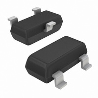
IC REG SHUNT ADJ 1.24V SOT23
Manufacturer
ON Semiconductor
Datasheet
1.TLV431ALPG.pdf
(14 pages)
Specifications of TLV431ASN1T1G
Reference Type
Shunt, Adjustable
Voltage - Output
1.24 ~ 16 V
Tolerance
±1%
Number Of Channels
1
Current - Cathode
55µA
Current - Output
20mA
Operating Temperature
-40°C ~ 85°C
Mounting Type
Surface Mount
Package / Case
SOT-23-3, TO-236-3, Micro3™, SSD3, SST3
Product
Voltage References
Topology
Shunt References
Output Voltage
Adjustable
Initial Accuracy
1 %
Series Vref - Input Voltage (max)
18 V
Shunt Current (max)
20 mA
Maximum Operating Temperature
+ 85 C
Minimum Operating Temperature
- 40 C
Mounting Style
SMD/SMT
Shunt Current (min)
0.08 mA
Fixed / Adjust / Prog
Adjust
Output Voltage (max)
1.24 to 16V
Reference Voltage Accuracy (max)
1
Input Voltage (max)
18V
Operating Temp Range
-40C to 85C
Operating Temperature Classification
Industrial
Mounting
Surface Mount
Pin Count
3
Package Type
SOT-23
Lead Free Status / RoHS Status
Lead free / RoHS Compliant
Voltage - Input
-
Temperature Coefficient
-
Current - Quiescent
-
Lead Free Status / Rohs Status
Lead free / RoHS Compliant
Other names
TLV431ASN1T1GOS
TLV431ASN1T1GOS
TLV431ASN1T1GOSTR
TLV431ASN1T1GOS
TLV431ASN1T1GOSTR
Available stocks
Company
Part Number
Manufacturer
Quantity
Price

Part Number:
TLV431ASN1T1G
Manufacturer:
ON/安森美
Quantity:
20 000


Stresses exceeding Maximum Ratings may damage the device. Maximum Ratings are stress ratings only. Functional operation above the
Recommended Operating Conditions is not implied. Extended exposure to stresses above the Recommended Operating Conditions may affect
device reliability.
NOTE:
MAXIMUM RATINGS
RECOMMENDED OPERATING CONDITIONS
Reference (R)
Cathode to Anode Voltage
Cathode Current
Cathode to Anode Voltage
Cathode Current Range, Continuous
Reference Input Current Range, Continuous
Thermal Characteristics
Operating Junction Temperature
Operating Ambient Temperature Range
Storage Temperature Range
LP Suffix Package, TO−92−3 Package
SN Suffix Package, TSOP−5 Package
SN1 Suffix Package, SOT−23−3 Package
Thermal Resistance, Junction−to−Ambient
Thermal Resistance, Junction−to−Case
Thermal Resistance, Junction−to−Ambient
Thermal Resistance, Junction−to−Ambient
This device series contains ESD protection and exceeds the following tests: Human Body Model 2000 V per MIL−STD−883,
Method 3015. Machine Model Method 200 V.
Device Symbol
Cathode (K)
Anode (A)
P
D
(Full operating ambient temperature range applies, unless otherwise noted)
+
T
Figure 2. Representative Device Symbol and Schematic Diagram
J(max)
R
qJA
Condition
Rating
* T
Reference (R)
A
http://onsemi.com
2
The device contains 13 active transistors.
Cathode (K)
Anode (A)
Symbol
Symbol
V
R
R
R
R
I
V
T
KA
K
I
T
T
I
ref
qJA
qJC
qJA
qJA
stg
KA
K
A
J
Min
V
0.1
ref
*0.05 to 10
*65 to 150
*40 to 85
−20 to 25
Value
178
226
491
150
18
83
Max
16
20
Unit
mA
mA
C/W
V
C
C
C
Unit
mA
V
Related parts for TLV431ASN1T1G
Image
Part Number
Description
Manufacturer
Datasheet
Request
R

Part Number:
Description:
ON Semiconductor [VOLTAGE REGULATOR]
Manufacturer:
ON Semiconductor
Datasheet:
Part Number:
Description:
357-036-542-201 CARDEDGE 36POS DL .156 BLK LOPRO
Manufacturer:
ON Semiconductor
Datasheet:
Part Number:
Description:
357-036-542-201 CARDEDGE 36POS DL .156 BLK LOPRO
Manufacturer:
ON Semiconductor
Datasheet:
Part Number:
Description:
357-036-542-201 CARDEDGE 36POS DL .156 BLK LOPRO
Manufacturer:
ON Semiconductor
Datasheet:
Part Number:
Description:
357-036-542-201 CARDEDGE 36POS DL .156 BLK LOPRO
Manufacturer:
ON Semiconductor
Datasheet:
Part Number:
Description:
357-036-542-201 CARDEDGE 36POS DL .156 BLK LOPRO
Manufacturer:
ON Semiconductor
Datasheet:
Part Number:
Description:
357-036-542-201 CARDEDGE 36POS DL .156 BLK LOPRO
Manufacturer:
ON Semiconductor
Datasheet:
Part Number:
Description:
357-036-542-201 CARDEDGE 36POS DL .156 BLK LOPRO
Manufacturer:
ON Semiconductor
Datasheet:
Part Number:
Description:
357-036-542-201 CARDEDGE 36POS DL .156 BLK LOPRO
Manufacturer:
ON Semiconductor
Datasheet:
Part Number:
Description:
357-036-542-201 CARDEDGE 36POS DL .156 BLK LOPRO
Manufacturer:
ON Semiconductor
Datasheet:
Part Number:
Description:
357-036-542-201 CARDEDGE 36POS DL .156 BLK LOPRO
Manufacturer:
ON Semiconductor
Datasheet:
Part Number:
Description:
Manufacturer:
ON Semiconductor
Datasheet:
Part Number:
Description:
Manufacturer:
ON Semiconductor
Datasheet:
Part Number:
Description:
Manufacturer:
ON Semiconductor
Datasheet: