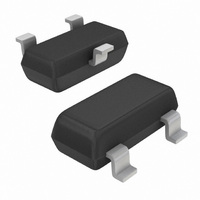
TLV431ASN1T1G ON Semiconductor, TLV431ASN1T1G Datasheet - Page 10

TLV431ASN1T1G
Manufacturer Part Number
TLV431ASN1T1G
Description
IC REG SHUNT ADJ 1.24V SOT23
Manufacturer
ON Semiconductor
Datasheet
1.TLV431ALPG.pdf
(14 pages)
Specifications of TLV431ASN1T1G
Reference Type
Shunt, Adjustable
Voltage - Output
1.24 ~ 16 V
Tolerance
±1%
Number Of Channels
1
Current - Cathode
55µA
Current - Output
20mA
Operating Temperature
-40°C ~ 85°C
Mounting Type
Surface Mount
Package / Case
SOT-23-3, TO-236-3, Micro3™, SSD3, SST3
Product
Voltage References
Topology
Shunt References
Output Voltage
Adjustable
Initial Accuracy
1 %
Series Vref - Input Voltage (max)
18 V
Shunt Current (max)
20 mA
Maximum Operating Temperature
+ 85 C
Minimum Operating Temperature
- 40 C
Mounting Style
SMD/SMT
Shunt Current (min)
0.08 mA
Fixed / Adjust / Prog
Adjust
Output Voltage (max)
1.24 to 16V
Reference Voltage Accuracy (max)
1
Input Voltage (max)
18V
Operating Temp Range
-40C to 85C
Operating Temperature Classification
Industrial
Mounting
Surface Mount
Pin Count
3
Package Type
SOT-23
Lead Free Status / RoHS Status
Lead free / RoHS Compliant
Voltage - Input
-
Temperature Coefficient
-
Current - Quiescent
-
Lead Free Status / Rohs Status
Lead free / RoHS Compliant
Other names
TLV431ASN1T1GOS
TLV431ASN1T1GOS
TLV431ASN1T1GOSTR
TLV431ASN1T1GOS
TLV431ASN1T1GOSTR
Available stocks
Company
Part Number
Manufacturer
Quantity
Price
Part Number:
TLV431ASN1T1G
Manufacturer:
ON/安森美
Quantity:
20 000
The above circuit shows the TLV431A/B as a compensated amplifier controlling the feedback loop of an isolated output line
powered switching regulator. The output voltage is programmed to 3.3 V by the resistors values selected for R1 and R2. The
minimum output voltage that can be programmed with this circuit is 2.64 V, and is limited by the sum of the reference voltage
(1.24 V) and the forward drop of the optocoupler light emitting diode (1.4 V). Capacitor C1 provides loop compensation.
ALYWWG
1
TO−92
TLV43
1XXX
G
2 3
AC Input
1. Reference
2. Anode
3. Cathode
Figure 31. Isolated Output Line Powered Switching Power Supply
Gate Drive
Controller
GND
Current
Sense
XXX
A
Y
L
WW, W = Work Week
G
(Note: Microdot may be in either location)
V
V
CC
FB
PIN CONNECTIONS AND DEVICE MARKING
= Specific Device Code
= Assembly Location
= Year
= Wafer Lot
= Pb−Free Package
Cathode
NC
NC
http://onsemi.com
1
2
3
(Top View)
TSOP−5
10
5
4
Anode
Reference
XXX
M
G
(Note: Microdot may be in either location)
Reference
100
Cathode
= Specific Device Code
= Date Code
= Pb−Free Package
C1
0.1 mF
SOT−23−3
1
2
(Top View)
R1
3.0 k
R2
1.8 k
3
DC Output
3.3 V
Anode


