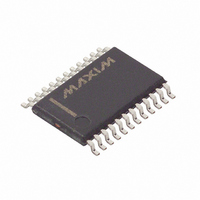
DS1780E Maxim Integrated Products, DS1780E Datasheet - Page 7

DS1780E
Manufacturer Part Number
DS1780E
Description
IC CPU PERIPHERAL MON 24-TSSOP
Manufacturer
Maxim Integrated Products
Datasheet
1.DS1780E.pdf
(28 pages)
Specifications of DS1780E
Function
Thermal Monitor, CPU Peripherals
Topology
ADC (Sigma Delta), Comparator, Fan Speed Control, Register Bank
Sensor Type
Internal
Sensing Temperature
-40°C ~ 125°C
Output Type
I²C™/SMBus™
Output Alarm
No
Output Fan
Yes
Voltage - Supply
2.8 V ~ 5.75 V
Operating Temperature
-40°C ~ 125°C
Mounting Type
Surface Mount
Package / Case
24-TSSOP
Full Temp Accuracy
+/- 12 %
Digital Output - Bus Interface
Serial (2-Wire)
Digital Output - Number Of Bits
8 bit
Maximum Operating Temperature
+ 125 C
Minimum Operating Temperature
- 40 C
Lead Free Status / RoHS Status
Contains lead / RoHS non-compliant
Available stocks
Company
Part Number
Manufacturer
Quantity
Price
Company:
Part Number:
DS1780E
Manufacturer:
MAX
Quantity:
3 000
Part Number:
DS1780E
Manufacturer:
DALLAS
Quantity:
20 000
Part Number:
DS1780E+T&R
Manufacturer:
MAXIM/美信
Quantity:
20 000
Company:
Part Number:
DS1780E+TR
Manufacturer:
MAXIM
Quantity:
1 001
Company:
Part Number:
DS1780E-TR
Manufacturer:
ICS
Quantity:
933
Company:
Part Number:
DS1780E/TR
Manufacturer:
XILINX
Quantity:
17
Software Reset - This condition is generated by writing a 1 to bit 4 of the configuration register. It has no
effect on DS1780 register contents. It will however pull the
duration of 20 ms (minimum). When the
clear itself. A Software Reset is only possible if Bit 7 of the INT Mask Register 2 (0x44h) is set to “1”.
Device Initialization - This condition is generated by writing a 1 to bit 7 of the configuration register. It
will clear all registers in DS1780 memory to their default state except the Value RAM (0x20h - 0x3Dh)
and analog output (0x19h). These locations will remain unchanged from their state before the
initialization. This condition has no effect on the
Hardware Reset - This condition is generated by some external source pulling the
VIN(0) (see DC Electrical Characteristics). The DS1780 will then force the
active low state for >20 ms. It will clear all registers in DS1780 memory to their default state except the
Value RAM (0x20h - 0x3Dh) and analog output (0x19h). These locations will remain unchanged from
their state before the Hardware Reset.
OPERATION - Configuration Register
Control of the DS1780 is provided through the configuration register. The Configuration Register is used
to start and stop the DS1780, enable or disable interrupt output and modes, and provide the initialization
function described above.
Bit 0 of the Configuration Register controls the monitoring loop of the DS1780. Setting Bit 0 low stops
the monitoring loop and puts the DS1780 into a standby mode. 2-Wire Bus communication is still
possible with any register in the DS1780 during the standby mode, however. Additionally, the DS1780
will continue to monitor the
monitoring loop.
Bit 1 of the Configuration Register enables or disables the
enables the
Bit 3 of the Configuration Register is used to clear the
monitoring function will stop until bit 3 is set low. Interrupt Status register contents will not be affected.
Bit 4 of the Configuration Register is used to initiate a minimum 20 ms RESET signal on the
if the pin is configured for the RESET mode (via bit 7 of the
Bit 6 of the Configuration Register is used to reset the Chassis Intrusion (CHS) output pin when set high.
Bit 7 of the Configuration Register is used to start a Configuration Register Initialization when taken
high, as described in the “OPERATION - Resets” section.
OPERATION - Monitoring Loop
The DS1780 monitoring function is started by doing a write to the Configuration Register and setting the
INT_Clear (Bit 3) low, and Start (Bit 0) high. At this point the INT_Enable (Bit 1) should be set high to
enable interrupts (INT). The DS1780 then performs a “round robin” sampling of the inputs, sampling
each approximately once a second, in the order (corresponding to locations in the Value RAM) shown
below in Table 3. The results of the sampling and conversions can be found in the Value RAM (Table
10.13) and are available at any time.
INT
output, setting bit 1 low disables the output.
RST
and CHS inputs while in a standby mode. Setting Bit 0 high starts the
RST
output goes active, this bit in the configuration register will
RST
7 of 28
output. This bit is self-clearing.
INT
interrupt output when set high. The DS1780
INT
INT
RST
Mask Register 2 - 0x44h).
Interrupt output. Setting Bit 1 high
output to the active low state for a
RST
signal to remain in the
RST
RST
pin below
output


