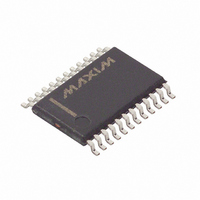
DS1780E Maxim Integrated Products, DS1780E Datasheet - Page 4

DS1780E
Manufacturer Part Number
DS1780E
Description
IC CPU PERIPHERAL MON 24-TSSOP
Manufacturer
Maxim Integrated Products
Datasheet
1.DS1780E.pdf
(28 pages)
Specifications of DS1780E
Function
Thermal Monitor, CPU Peripherals
Topology
ADC (Sigma Delta), Comparator, Fan Speed Control, Register Bank
Sensor Type
Internal
Sensing Temperature
-40°C ~ 125°C
Output Type
I²C™/SMBus™
Output Alarm
No
Output Fan
Yes
Voltage - Supply
2.8 V ~ 5.75 V
Operating Temperature
-40°C ~ 125°C
Mounting Type
Surface Mount
Package / Case
24-TSSOP
Full Temp Accuracy
+/- 12 %
Digital Output - Bus Interface
Serial (2-Wire)
Digital Output - Number Of Bits
8 bit
Maximum Operating Temperature
+ 125 C
Minimum Operating Temperature
- 40 C
Lead Free Status / RoHS Status
Contains lead / RoHS non-compliant
Available stocks
Company
Part Number
Manufacturer
Quantity
Price
Company:
Part Number:
DS1780E
Manufacturer:
MAX
Quantity:
3 000
Part Number:
DS1780E
Manufacturer:
DALLAS
Quantity:
20 000
Part Number:
DS1780E+T&R
Manufacturer:
MAXIM/美信
Quantity:
20 000
Company:
Part Number:
DS1780E+TR
Manufacturer:
MAXIM
Quantity:
1 001
Company:
Part Number:
DS1780E-TR
Manufacturer:
ICS
Quantity:
933
Company:
Part Number:
DS1780E/TR
Manufacturer:
XILINX
Quantity:
17
A CHS (Chassis Intrusion) digital input is provided. The Chassis Intrusion input is designed to accept an
active high signal from an external circuit that latches when the case is removed from the computer; this
pin is a dual purpose pin which will be driven low by the DS1780 to reset the external circuit.
DS1780 FUNCTIONAL BLOCK DIAGRAM Figure 1
Note: R1 and R2 on the -12V resistance ladder should be ratioed such that approximately +2.5V appears
at the input pin (i.e., R1=4kΩ, R2=23.2 kΩ). If a second processor voltage needs to be monitored (V
leave R2 empty, and make R1 500Ω, with V
2-WIRE SERIAL DATA BUS
When using the 2-wire bus, a write will always consist of the DS1780 2-wire slave address, followed by
the Internal Address Register byte, then the data byte. The Internal Address Register addresses are listed
below in Table 2. There are two cases for a read:
1. If the Internal Address Register is known to be at the desired Address, simply read the DS1780 with
2. If the Internal Address Register value is unknown, write to the DS1780 with the 2-wire slave address,
The default power-on 2-wire slave address for the DS1780 is 01011(A1)(A0) binary, where A0-A1
reflects the state of the pins defined by the same names. The address can be changed by writing any
desired value to the 2-wire Serial Address Register (excluding the 2 LSBs). This communication protocol
is depicted in the 2-wire timing diagrams of Figures 2 and 8.
the 2-wire slave address, followed by the data byte read from the DS1780.
followed by the Internal Address Register byte. Then restart the Serial Communication with a Read
consisting of the 2-wire slave address, followed by the data byte read from the DS1780.
CCP2
appearing here.
4 of 28
CCP2
),


