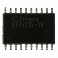
BTS5235-2G Infineon Technologies, BTS5235-2G Datasheet - Page 21

BTS5235-2G
Manufacturer Part Number
BTS5235-2G
Description
IC PWR SWITCH HISIDE PGDSO-20-43
Manufacturer
Infineon Technologies
Type
High Sider
Datasheet
1.BTS5235-2G.pdf
(25 pages)
Specifications of BTS5235-2G
Package / Case
DSO-20
Input Type
Non-Inverting
Number Of Outputs
2
On-state Resistance
45 mOhm
Current - Output / Channel
3.3A
Current - Peak Output
28A
Voltage - Supply
4.5 V ~ 28 V
Operating Temperature
-40°C ~ 150°C
Mounting Type
Surface Mount
On Resistance (max)
0.045 Ohms
Maximum Operating Temperature
+ 150 C
Minimum Operating Temperature
- 40 C
Maximum Power Dissipation
1400 mW
Mounting Style
SMD/SMT
Supply Current
3.6 mA
Lead Free Status / RoHS Status
Lead free / RoHS Compliant
Lead Free Status / RoHS Status
Lead free / RoHS Compliant, Lead free / RoHS Compliant
Other names
BTS5235-2GINTR
BTS52352GXT
SP000281079
BTS52352GXT
SP000281079
Available stocks
Company
Part Number
Manufacturer
Quantity
Price
Part Number:
BTS5235-2G
Manufacturer:
INFINEON/英飞凌
Quantity:
20 000
7.3
The diagnosis signals have to be switched on by a high signal at sense enable pin (SEN). See
on the timing between SEN pin and diagnosis signal I
is provided at pin SEN.
Figure 18
The SEN pin circuit is designed equally to the input pin. Please refer to
recommended to limit the current through the sense pins IS1 and IS2 in case of reverse polarity and over voltage.
Please refer to maximum ratings on
The stand-by current of the BTS5235-2G is minimized, when both input pins (IN1 and IN2) and the sense enable
pin (SEN) are on low level.
7.4
V
typical values:
Pos. Parameter
General Definition
7.4.1 Diagnostics signal in failure mode
7.4.2 Diagnostics signal current limitation in failure
Open Load at OFF-State
7.4.3 Open load detection threshold voltage
7.4.4 Sense signal invalid after negative input slope t
7.4.5 Fault signal settling time
Data Sheet
bb
= 9 V to 16 V,
SEN
mode
I
IS
Sense Enable Function
Timing of Sense Enable Signal
Electrical Characteristics
t
sIS(SEN)
V
bb
T
= 13.5 V,
j
= -40 C to +150 C,
T
j
= 25 C
t
dIS(SEN)
Page
V
8.
SEN
= 5 V, (unless otherwise specified)
IS
. Please note that the diagnosis is disabled, when no signal
Symbol
V
I
V
t
21
d(fault)
s(fault)
IS(LIM)
IS(fault)
OUT(OL)
t
sIS(SEN)
min. typ. max.
1.6
5
3
–
–
Limit Values
Figure 5
2.8
Smart High-Side Power Switch
–
–
–
–
200
4.4
1.2
9
–
for details. The resistors R
t
dIS(SEN)
Unit
V
mA
V
ms
s
Rev.1.1, 2007-09-01
Conditions
V
V
I
V
V
V
V
V
V
I
Figure 18
IS
IS
IN
OUT
IN
OUT
IN
OUT
IN
OUT
t
t
= 1 mA
> V
= 1 mA
= 0 V
= 0 V
= 5 V to 0 V
= 0 V
BTS5235-2G
= V
= V
= V
= 0 V to
OUT(OL)
SEN.emf
bb
bb
bb
Diagnosis
for details
lim
are


