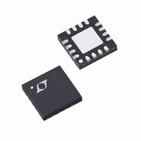
LTC5100EUF Linear Technology, LTC5100EUF Datasheet - Page 7

LTC5100EUF
Manufacturer Part Number
LTC5100EUF
Description
IC DRIVER VCSEL 3.2GBPS 16QFN
Manufacturer
Linear Technology
Type
Laser Diode Driverr
Datasheet
1.LTC5100EUF.pdf
(52 pages)
Specifications of LTC5100EUF
Data Rate
3.2Gbps
Number Of Channels
1
Voltage - Supply
3.135 V ~ 3.465 V
Current - Supply
54mA
Current - Modulation
12mA
Operating Temperature
-40°C ~ 85°C
Package / Case
16-QFN
Mounting Type
Surface Mount
Lead Free Status / RoHS Status
Contains lead / RoHS non-compliant
Available stocks
Company
Part Number
Manufacturer
Quantity
Price
Company:
Part Number:
LTC5100EUF
Manufacturer:
LT
Quantity:
10 000
Part Number:
LTC5100EUF
Manufacturer:
LINEAR/凌特
Quantity:
20 000
Company:
Part Number:
LTC5100EUF#PBF
Manufacturer:
LT
Quantity:
5 000
Part Number:
LTC5100EUF#PBF
Manufacturer:
LINEAR/凌特
Quantity:
20 000
Note 10: The modulation current can be programmed to near zero in each
range, but the high speed performance is not guaranteed for currents less
than the specified minimum.
Note 11: The effective resolution of the modulation current is 9 bits
because the modulation servo system uses only one-half of the 10-bit
ADC range.
Note 12: As defined in ANSI x3.230, Annex A, deterministic jitter is the
peak-to-peak deviation of the 50% crossings of the modulation signal
when compared to the ideal time crossings. The specification for the
LTC5100 pertains to the electrical modulation signal. The K28.5 pattern is
the repeating sequence 00111110101100000101.
Note 13: Random jitter is the standard deviation of the 50% crossings of
the electrical modulation signal as measured by an oscilloscope. It is
measured with a 1GHz square wave after quadrature subtraction of the
random jitter of the pulse generator and oscilloscope. Peak-to-peak
random jitter is defined as 14 times the RMS random jitter.
Note 14: The LTC5100 digitizes and servo controls the logarithm of the
monitor diode current. Many of the characteristics of the APC system,
such as range and resolution, are determined by the ADC.
Note 15: The minimum practical operating current for the monitor diode is
determined by servo settling time considerations.
ELECTRICAL CHARACTERISTICS
Note 16: I
corresponding to Imd_rng = 0, 1, 2, 3.
Note 17: The temperature coefficients of the monitor diode current depend
on the I
point and the monitor diode current. Imd_nom is the digital code setting
for the nominal monitor diode current. Imd_nom lies between 0 and 1023.
Note 18: The ADC digitizes the average modulation current, which is 50%
of the peak-to-peak current for a 50% duty cycle signal.
Note 19: The LTC5100 ADC digitizes the logarithm of the monitor diode
current. This implies that the ADC resolution is a constant percentage of
reading and that the monitor diode current is non-zero when the ADC
reads zero. See the Design Notes for further information.
Note 20: Serial interface timing is guaranteed by design from
–40 C to 85 C.
Note 21: The LTC5100 has 100 A nominal pull-up current sources on the
SCL and SDA pins to eliminate the need for external pull-up resistors when
connected to a single EEPROM device. The LTC5100 meets the maximum
rise time specification of 1000ns with external I
25pF. Example: 10pF EEPROM + 150mm trace ~ 25pF.
Note 22: V
MD
MD
DD
setting because of the logarithmic relationship between the set
must be less than 25 A, 100 A, 400 A and 1600 A
and V
DD(HS)
must be tied together on the PC board.
2
C bus capacitances up to
LTC5100
sn5100 5100fs
7


