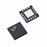
LTC5100EUF Linear Technology, LTC5100EUF Datasheet - Page 2

LTC5100EUF
Manufacturer Part Number
LTC5100EUF
Description
IC DRIVER VCSEL 3.2GBPS 16QFN
Manufacturer
Linear Technology
Type
Laser Diode Driverr
Datasheet
1.LTC5100EUF.pdf
(52 pages)
Specifications of LTC5100EUF
Data Rate
3.2Gbps
Number Of Channels
1
Voltage - Supply
3.135 V ~ 3.465 V
Current - Supply
54mA
Current - Modulation
12mA
Operating Temperature
-40°C ~ 85°C
Package / Case
16-QFN
Mounting Type
Surface Mount
Lead Free Status / RoHS Status
Contains lead / RoHS non-compliant
Available stocks
Company
Part Number
Manufacturer
Quantity
Price
Company:
Part Number:
LTC5100EUF
Manufacturer:
LT
Quantity:
10 000
Part Number:
LTC5100EUF
Manufacturer:
LINEAR/凌特
Quantity:
20 000
Company:
Part Number:
LTC5100EUF#PBF
Manufacturer:
LT
Quantity:
5 000
Part Number:
LTC5100EUF#PBF
Manufacturer:
LINEAR/凌特
Quantity:
20 000
ABSOLUTE AXI U RATI GS
LTC5100
(Note 1)
V
IN
IN
Cml_en = 0 (Note 4)
MODA, MODB (Transmitter Disabled) .... –0.3V to 2.75V
MODA, MODB
(Transmitter Enabled) ............ V
EN, SDA, SCL, FAULT ..................... –0.3V to V
MD, SRC ................................................... –0.3V to V
Ambient Operating Temperature Range .. – 40 C to 85 C
Storage Temperature Range ................ – 65 C to 125 C
temperature range, otherwise specifications are at T
resistor from SRC (Pin 14) to MODA (Pin 11); 50 , 1% load AC coupled to MODB (Pin 10); 10nF, 10% capacitor from SRC (Pin 14) to
V
PARAMETER
Power Supply
V
V
Excluding the SRC Pin Current (Note 2)
High Speed Data Inputs (IN
Input Signal Amplitude
Common Mode Input Signal Range (Note 3)
Differential Input Resistance
Common Mode Input Resistance
Open-Circuit Voltage
SRC Pin Current, I
Full-Scale I
Minimum Operating Current (Note 7)
Resolution
SRC Pin Voltage Range
2
ELECTRICAL CHARACTERISTICS
DD
DD
SS
DD
+
+
Peak Voltage ........... V
Average Voltage...... V
Peak Difference Between IN
Average Difference Between IN
, V
, IN
, IN
; Cml_en = 0, Lpc_en = 1, transmitter enabled, unless otherwise noted. Test circuit in Figure 5.
+ V
, V
DD(HS)
DD(HS)
DD(HS)
–
–
(Cml_en = 1) (Note 6)
(Cml_en = 0) (Note 4) .. –0.3V to V
S
Current
Operating Voltage
Quiescent Current,
............................................................. 4V
S
W
+
and IN
DD(HS)
DD(HS)
W W
–
Pins) (Test Circuit, Figure 5)
+
– 1.2V to V
– 0.6V to V
and IN
DD(HS)
+
and IN
–
– 2.75V to 2.75V
.............. 2.5V
–
DD(HS)
DD(HS)
CONDITIONS
V
Transmitter Disabled, Power_down_en = 1
Transmitter Enabled, Is_rng = Im_rng = 3
Impp = 24mA
Peak-to-Peak Differential Voltage (The Single-
Ended Peak-to-Peak Voltage is One Half the
Differential Voltage)
Cml_en = 0 (Note 4)
Cml_en = 0 (Note 5)
Cml_en = 0 (Note 5)
Is_rng = 0
Is_rng = 1
Is_rng = 2
Is_rng = 3
DD(HS)
....... 1.25V
DD
U
A
= 3.465V
DD
= 25 C; V
+ 0.3V
+ 0.3V
+ 0.3V
+ 0.3V
The
DD
DD
denotes the specifications which apply over the full operating
= V
PACKAGE/ORDER I FOR ATIO
Consult LTC Marketing for parts specified with wider operating temperature ranges.
DD(HS)
MUST BE SOLDERED TO PCB GROUND PLANE
16-LEAD (4mm 4mm) PLASTIC QFN
V
V
IN
IN
= 3.3V, I
SS
SS
+
–
EXPOSED PAD IS V
T
JMAX
1
2
3
4
16 15 14 13
5
= 125 C,
UF PACKAGE
TOP VIEW
S
6
= 24mA; I
17
7
JA
SS
= 37 C/W
8
(PIN 17)
12
11
10
9
M
= 12mA (I
V
MODA
MODB
V
SS
SS
1/16 of Full-Scale I
3.135
MIN
1.2
12
18
24
0
6
U
500 to 2400
MPP
80 to 120
UF PART MARKING
1.65
TYP
ORDER PART
3.3
4.5
54
50
18
27
36
10
= 24mA); 49.9 , 1%
9
LTC5100EUF
NUMBER
W
S
5100
Current
V
200mV
3.465
V
MAX
DD(HS)
DD
–
sn5100 5100fs
UNITS
mV
U
Bits
mA
mA
mA
mA
mA
mA
P-P
k
V
V
V
V


