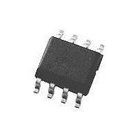
M25P40-VMP6TG NUMONYX, M25P40-VMP6TG Datasheet - Page 22

M25P40-VMP6TG
Manufacturer Part Number
M25P40-VMP6TG
Description
IC FLASH 4MBIT 50MHZ 8VFQFPN
Manufacturer
NUMONYX
Series
Forté™r
Datasheet
1.M25P40-VMP6G.pdf
(61 pages)
Specifications of M25P40-VMP6TG
Format - Memory
FLASH
Memory Type
FLASH
Memory Size
4M (512K x 8)
Speed
50MHz
Interface
SPI, 3-Wire Serial
Voltage - Supply
2.3 V ~ 3.6 V
Operating Temperature
-40°C ~ 85°C
Package / Case
8-VFQFN, 8-VFQFPN
Memory Configuration
512K X 8
Ic Interface Type
Serial, SPI
Clock Frequency
50MHz
Supply Voltage Range
2.3V To 3.6V
Memory Case Style
VDFPN
No. Of Pins
8
Lead Free Status / RoHS Status
Lead free / RoHS Compliant
Available stocks
Company
Part Number
Manufacturer
Quantity
Price
Company:
Part Number:
M25P40-VMP6TG
Manufacturer:
st
Quantity:
11 116
Part Number:
M25P40-VMP6TG
Manufacturer:
ST
Quantity:
20 000
Company:
Part Number:
M25P40-VMP6TG-X
Manufacturer:
STM
Quantity:
12 000
Part Number:
M25P40-VMP6TG-X
Manufacturer:
ST
Quantity:
20 000
Company:
Part Number:
M25P40-VMP6TG/TE
Manufacturer:
ST
Quantity:
2 000
6.4
6.4.1
6.4.2
22/61
Figure 9.
Read Status Register (RDSR)
The Read Status Register (RDSR) instruction allows the Status Register to be read. The
Status Register may be read at any time, even while a Program, Erase or Write Status
Register cycle is in progress. When one of these cycles is in progress, it is recommended to
check the Write In Progress (WIP) bit before sending a new instruction to the device. It is
also possible to read the Status Register continuously, as shown in
Table 6.
The status and control bits of the Status Register are as follows:
WIP bit
The Write In Progress (WIP) bit indicates whether the memory is busy with a Write Status
Register, Program or Erase cycle. When set to 1, such a cycle is in progress, when reset to
0 no such cycle is in progress.
WEL bit
The Write Enable Latch (WEL) bit indicates the status of the internal Write Enable Latch.
When set to 1 the internal Write Enable Latch is set, when set to 0 the internal Write Enable
Latch is reset and no Write Status Register, Program or Erase instruction is accepted.
Status Register Write Protect
S
C
D
Q
SRWD
b7
Read Identification (RDID) instruction sequence and data-out sequence
Status Register format
0
High Impedance
1
0
2
Instruction
3
4
5
0
6
7
MSB
Manufacturer Identification
8
BP2
9 10 11 12 13 14 15
BP1
Block Protect bits
MSB
15 14 13
16 17 18
Write Enable Latch bit
BP0
Device Identification
Figure
3
28 29 30 31
WEL
Write In Progress bit
2
10.
1
0
AI06809b
WIP
b0


