CY14B101L-SZ45XC Cypress Semiconductor Corp, CY14B101L-SZ45XC Datasheet - Page 10
CY14B101L-SZ45XC
Manufacturer Part Number
CY14B101L-SZ45XC
Description
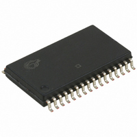
IC NVSRAM 1MBIT 45NS 32SOIC
Manufacturer
Cypress Semiconductor Corp
Type
NVSRAMr
Specifications of CY14B101L-SZ45XC
Memory Size
1M (128K x 8)
Package / Case
32-SOIC (7.5mm Width)
Interface
Parallel
Format - Memory
RAM
Memory Type
NVSRAM (Non-Volatile SRAM)
Speed
45ns
Voltage - Supply
2.7 V ~ 3.6 V
Operating Temperature
0°C ~ 70°C
Access Time
45ns
Supply Voltage Range
2.7V To 3.6V
Memory Case Style
SOIC
No. Of Pins
32
Operating Temperature Range
0°C To +70°C
Word Size
8b
Organization
128Kx8
Density
1Mb
Interface Type
Parallel
Access Time (max)
45ns
Operating Supply Voltage (typ)
3.3V
Package Type
SOIC
Operating Temperature Classification
Commercial
Operating Supply Voltage (max)
3.6V
Operating Supply Voltage (min)
2.7V
Operating Temp Range
0C to 70C
Pin Count
32
Mounting
Surface Mount
Supply Current
50mA
Memory Configuration
128K X 8
Rohs Compliant
Yes
Lead Free Status / RoHS Status
Lead free / RoHS Compliant
Lead Free Status / RoHS Status
Lead free / RoHS Compliant, Lead free / RoHS Compliant
Available stocks
Company
Part Number
Manufacturer
Quantity
Price

Part Number:
CY14B101L-SZ45XC
Manufacturer:
CYPRESS/赛普拉斯
Quantity:
20 000


AC Switching Characteristics
SRAM Read Cycle
Switching Waveforms
Document Number: 001-06400 Rev. *K
t
t
t
t
t
t
t
t
t
t
t
Notes
ACE
RC
AA
DOE
OHA
LZCE
HZCE
LZOE
HZOE
PU
PD
7. WE and HSB must be HIGH during SRAM READ cycles.
8. Device is continuously selected with CE and OE both Low.
9. Measured ±200 mV from steady state output voltage.
10. HSB must remain high during READ and WRITE cycles.
Parameter
Cypress
[8]
[7]
[6]
[6]
[8]
[9]
[9]
[9]
[9]
Parameter
t
t
t
t
t
t
t
t
t
t
t
ELQV
AVAV,
AVQV
GLQV
AXQX
ELQX
EHQZ
GLQX
GHQZ
ELICCH
EHICCL
t
ELEH
Alt
Chip Enable Access Time
Read Cycle Time
Address Access Time
Output Enable to Data Valid
Output Hold After Address Change
Chip Enable to Output Active
Chip Disable to Output Inactive
Output Enable to Output Active
Output Disable to Output Inactive
Chip Enable to Power Active
Chip Disable to Power Standby
Figure 6. SRAM Read Cycle 2: CE and OE Controlled
Figure 5. SRAM Read Cycle 1: Address Controlled
Description
Min
25
3
3
0
0
25 ns
Max
25
12
10
10
25
25
[7, 8, 10]
[7, 10]
Min
35
3
3
0
0
35 ns
Max
35
35
15
13
13
35
Min
45
3
0
0
3
CY14B101L
45 ns
Page 10 of 20
Max
45
45
20
15
15
45
Unit
ns
ns
ns
ns
ns
ns
ns
ns
ns
ns
ns
[+] Feedback
Related parts for CY14B101L-SZ45XC
Image
Part Number
Description
Manufacturer
Datasheet
Request
R

Part Number:
Description:
CY14B101L-SP45XC
Manufacturer:
Cypress Semiconductor Corp
Datasheet:

Part Number:
Description:
CY14B101L-SZ35XCT
Manufacturer:
Cypress Semiconductor Corp
Datasheet:
Part Number:
Description:
IC NVSRAM 1MBIT 35NS 32SOIC
Manufacturer:
Cypress Semiconductor Corp
Datasheet:
Part Number:
Description:
IC NVSRAM 1MBIT 35NS 48SSOP
Manufacturer:
Cypress Semiconductor Corp
Datasheet:
Part Number:
Description:
IC NVSRAM 1MBIT 35NS 32SOIC
Manufacturer:
Cypress Semiconductor Corp
Datasheet:
Part Number:
Description:
IC NVSRAM 1MBIT 45NS 32SOIC
Manufacturer:
Cypress Semiconductor Corp
Datasheet:
Part Number:
Description:
IC NVSRAM 1MBIT 45NS 48SSOP
Manufacturer:
Cypress Semiconductor Corp
Datasheet:
Part Number:
Description:
IC NVSRAM 1MBIT 35NS 48SSOP
Manufacturer:
Cypress Semiconductor Corp
Datasheet:
Part Number:
Description:
IC NVSRAM 1MBIT 35NS 48SSOP
Manufacturer:
Cypress Semiconductor Corp
Datasheet:
Part Number:
Description:
IC NVSRAM 1MBIT 35NS 48SSOP
Manufacturer:
Cypress Semiconductor Corp
Datasheet:
Part Number:
Description:
IC NVSRAM 1MBIT 45NS 48SSOP
Manufacturer:
Cypress Semiconductor Corp
Datasheet:
Part Number:
Description:
IC NVSRAM 1MBIT 45NS 48SSOP
Manufacturer:
Cypress Semiconductor Corp
Datasheet:
Part Number:
Description:
IC NVSRAM 1MBIT 35NS 32SOIC
Manufacturer:
Cypress Semiconductor Corp
Datasheet:
Part Number:
Description:
IC NVSRAM 1MBIT 45NS 32SOIC
Manufacturer:
Cypress Semiconductor Corp
Datasheet:
Part Number:
Description:
IC NVSRAM 1MBIT 45NS 32SOIC
Manufacturer:
Cypress Semiconductor Corp
Datasheet: