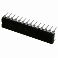
CY7C185-20PXC Cypress Semiconductor Corp, CY7C185-20PXC Datasheet - Page 5

CY7C185-20PXC
Manufacturer Part Number
CY7C185-20PXC
Description
IC SRAM 64KBIT 20NS 28DIP
Manufacturer
Cypress Semiconductor Corp
Type
Asynchronousr
Datasheet
1.CY7C185-20PXC.pdf
(12 pages)
Specifications of CY7C185-20PXC
Memory Size
64K (8K x 8)
Package / Case
28-DIP (0.300", 7.62mm)
Format - Memory
RAM
Memory Type
SRAM - Asynchronous
Speed
20ns
Interface
Parallel
Voltage - Supply
4.5 V ~ 5.5 V
Operating Temperature
0°C ~ 70°C
Access Time
20 ns
Supply Voltage (max)
5.5 V
Supply Voltage (min)
4.5 V
Maximum Operating Current
110 mA
Maximum Operating Temperature
+ 70 C
Minimum Operating Temperature
0 C
Mounting Style
Through Hole
Number Of Ports
1
Operating Supply Voltage
5 V
Memory Configuration
8K X 8
Supply Voltage Range
4.5V To 5.5V
Memory Case Style
DIP
No. Of Pins
28
Operating Temperature Range
0°C To +70°C
Rohs Compliant
Yes
Density
64Kb
Access Time (max)
20ns
Sync/async
Asynchronous
Architecture
Not Required
Clock Freq (max)
Not RequiredMHz
Operating Supply Voltage (typ)
5V
Address Bus
13b
Package Type
PDIP
Operating Temp Range
0C to 70C
Supply Current
110mA
Operating Supply Voltage (min)
4.5V
Operating Supply Voltage (max)
5.5V
Operating Temperature Classification
Commercial
Mounting
Through Hole
Pin Count
28
Word Size
8b
Number Of Words
8K
Lead Free Status / RoHS Status
Lead free / RoHS Compliant
Lead Free Status / RoHS Status
Lead free / RoHS Compliant, Lead free / RoHS Compliant
Other names
428-2157-5
CY7C185-20PXC
CY7C185-20PXC
Available stocks
Company
Part Number
Manufacturer
Quantity
Price
Company:
Part Number:
CY7C185-20PXC
Manufacturer:
MICRON
Quantity:
1 000
Switching Waveforms
Document #: 38-05043 Rev. *D
Notes
12. During this period, the IOs are in the output state and input signals must not be applied.
13. The minimum write cycle time for write cycle #3 (WE controlled, OE LOW) is the sum of t
ADDRESS
ADDRESS
DATA IO
DATA IO
CE
CE
CE
CE
WE
WE
OE
CE
1
2
1
2
NOTE 12
(continued)
t
SA
t
HZOE
Figure 5. Write Cycle No. 2 (CE Controlled)
Figure 4. Write Cycle No. 1 (WE Controlled)
t
SA
t
AW
t
AW
t
SCE2
t
SCEI
t
t
WC
WC
DATA
t
PWE
t
DATA
SD
IN
t
t
SCE1
SCE2
VALID
t
HZWE
SD
IN
VALID
and t
SD
[11,12,13]
.
[9,11]
t
HD
t
HA
t
HD
t
HA
CY7C185
Page 5 of 12
[+] Feedback


