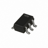
74LVC1G18GW,125 NXP Semiconductors, 74LVC1G18GW,125 Datasheet - Page 7

74LVC1G18GW,125
Manufacturer Part Number
74LVC1G18GW,125
Description
IC 1OF2 NON-INV DEMUX 3ST SC-88
Manufacturer
NXP Semiconductors
Series
74LVCr
Type
Demultiplexerr
Datasheet
1.74LVC1G18GV125.pdf
(13 pages)
Specifications of 74LVC1G18GW,125
Package / Case
SC-70-6, SC-88, SOT-363
Circuit
1 x 1:2
Independent Circuits
1
Current - Output High, Low
32mA, 32mA
Voltage Supply Source
Single Supply
Voltage - Supply
1.65 V ~ 5.5 V
Operating Temperature
-40°C ~ 125°C
Mounting Type
Surface Mount
Logic Family
LVC
Number Of Lines (input / Output)
1.0 / 2.0
Propagation Delay Time
50 ns
Supply Voltage (max)
5.5 V
Supply Voltage (min)
1.65 V
Maximum Operating Temperature
+ 125 C
Minimum Operating Temperature
- 40 C
Mounting Style
SMD/SMT
Number Of Input Lines
1.0
Number Of Output Lines
2.0
Lead Free Status / RoHS Status
Lead free / RoHS Compliant
Lead Free Status / RoHS Status
Lead free / RoHS Compliant, Lead free / RoHS Compliant
Other names
74LVC1G18GW-G
74LVC1G18GW-G
935273781125
74LVC1G18GW-G
935273781125
NXP Semiconductors
12. AC waveforms
Table 9.
74LVC1G18_2
Product data sheet
V
1.65 V to 1.95 V
2.3 V to 2.7 V
2.7 V
3.0 V to 3.6 V
4.5 V to 5.5 V
Fig 3. Input A to output Y propagation delays
Fig 4. 3-state enable and disable times
CC
Measurement points are given in
Measurement points are given in
V
V
V
V
X
X
Y
Y
Measurement points
= V
= V
= V
= V
OL
OL
OH
OH
+ 0.3 V at V
+ 0.15 V at V
0.3 V at V
0.15 V at V
HIGH-to-OFF
OFF-to-HIGH
CC
OFF-to-LOW
LOW-to-OFF
CC
CC
CC
nY output
nY output
S input
V
0.5
0.5
1.5 V
1.5 V
0.5
< 2.7 V.
< 2.7 V.
M
2.7 V.
2.7 V.
nY output
V
V
V
CC
CC
CC
A input
Table
Table
GND
GND
V OH
V CC
V OL
V
I
9. V
9. V
GND
V
V
1-of-2 non-inverting demultiplexer with 3-state deselected output
OH
OL
OL
OL
V
I
Rev. 02 — 30 August 2007
and V
enabled
and V
V
M
output
t
PLZ
t
PHZ
OH
OH
are typical output voltage levels that occur with the output load.
are typical output voltage levels that occur with the output load.
V
V
M
X
V M
V
Input
V
V
V
2.7 V
2.7 V
V
Y
I
CC
CC
CC
t
PHL
disabled
output
V
t
M
PZL
t
PZH
V
mnb089
M
t
PLH
V
M
V
M
enabled
output
mnb090
t
r
2.0 ns
2.0 ns
2.5 ns
2.5 ns
2.5 ns
= t
74LVC1G18
f
© NXP B.V. 2007. All rights reserved.
7 of 13


